AN-2622: Selecting an Analog Devices RF Low Noise Amplifier
Introduction
Figure 1 shows the frequency response of HMC8413, a 10MHz to 9GHz low noise amplifier (LNA). In addition to gain and noise figure, the plot also includes compression, second order and third order distortion. The device exhibits a flat response across more than six octaves. All key LNA specifications—including gain, compression, and distortion—impact system performance, not just noise figure and frequency range. Selecting an RF LNA is challenging because multiple interdependent specifications must be evaluated simultaneously. In addition, it can be difficult to differentiate all of the devices in the LNA portfolio of Analog Devices Inc. with more than 200 generics.


This application note explains how to select an RF LNA from Analog Devices’ large and diverse portfolio of RF LNAs. It begins with an overview of the Analog Devices portfolio. This includes a discussion of the relative vintage of different product families and guidelines on part number nomenclature. From there, various considerations that affect the choice of LNA are discussed. The document is structured so that it can be read from start to finish or can be used as a reference source on specific topics.
What Is the Difference Between Depletion Mode and Single Positive Supply Enhancement Mode LNAs?
One fundamental differentiator between LNAs from Analog Devices is how they are biased, specifically how the quiescent operating current is set. LNAs that are fabricated on depletion mode processes, have a drain to source (or VDD to ground) resistance of almost 0Ω when the gate voltage is open or equal to 0V (see Figure 2). This low resistance between VDD and ground can be physically measured using an ohmmeter and is often mistaken as an indicator that the device is damaged or destroyed.


A negative gate voltage must be applied to bias on the main transistor. This voltage is typically between −0.5V and −2V and must be carefully sequenced so that it is applied before VDD turns on and removed after VDD turns off.
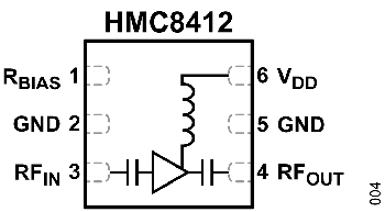
Figure 3 shows the application circuit for a typical enhancement mode LNA. In this case, the operating bias current is set by connecting a resistor between the RBIAS pin and VDD. All newer LNAs from Analog Devices use this circuit architecture and have part numbers with the format HMC841X, ADL7XXX, and ADL8XXX (for example, HMC8414, ADL7078, and ADL8100). Power supply sequencing is not critical and because there is no need for a negative supply voltage, these LNAs are easier to use than depletion mode devices.


There are also a class of older LNAs that have a fixed bias setting. These devices typically have a single positive supply voltage and a fixed quiescent bias current that cannot be adjusted.
The Analog Devices LNA Portfolio
Analog Devices portfolio of LNAs is a combination of multiple product portfolios developed or acquired over time. The family of approximately 200 devices is summarized in Table 1 with the newer devices and product families at the top and the older devices at the bottom.
| Part Numbering | Frequency Coverage | Frequency Bands | Target End Applications | Example | Comments | Approximate Number of Generics |
| ADL81XX | 10MHz to 54GHz | VHF to V | General purpose | ADL8100 | Single supply with RBIAS | 20 |
| ADL7XXX | 1GHz to 20GHz, 50GHz to 95GHz | L to KU, V, E | General purpose | ADL7078 | 2 | |
| ADL900X | 10 MHz to 28GHz | VHF to K | General purpose | ADL9005 | Single supply | 4 |
| HMC841X | 10MHz to 11GHz | HF to X | General purpose | HMC8411 | Single supply with RBIAS | 9 |
| HMC840X | 10MHz to 30GHz | HF to K | General purpose | HMC8400-DIE | Requires negative gate voltage | 3 |
| ADL8111X, HMC8414 | 10MHz to 25.5GHz | HF to K | High dynamic range receivers, bidirectional circuits, test and measurement equipment | ADL8113 | LNA with bypass and bidirectional operation, single supply with RBIAS | 4 |
| ADLXXXX-CSL, ADLXXXX-CSH | 30KHz to 31GHz | LF to KA | Commercial space low, commercial space high | ADL8141- CSL | Single supply with RBIAS | 5 |
| ADHXXXS | 10MHz to 65GHz | HF to V | Traditional space | ADH903S | QMLV space qualified | 18 |
| ADL57XX | 6GHz to 24GHz | C, X, KU, K | Differential Rx mixer driver, ADC driver | ADL5721 | Single-ended to differential amp, single supply | 5 |
| MAX-XXXX | 40MHz to 4GHz | VHF, UHF, L, S | GPS/GNSS, automotive FM radio, general purpose | MAX2694 | Single supply silicon based devices | 40 |
| HMC-ALHXXX | 500MHz to 86MHz | L to E | General purpose | HMCALH244-DIE | Older portfolio, die product only | 15 |
| HMC1XXX,HMC2XX, HMC3XX, HMC4XX, HMC5XX, HMC6XX, HMC7XX, HMC9XXX, ADL55XX |
30KHz to 36GHz | LF to V | General purpose | HMC1126, ADL5521 | Older portfolio, mostly require negative gate voltage | 57 |
Newer devices (for example those with part numbers ADL8XXX, ADL7XXX, and HMC8XXX) tend to be broadband, internally matched and operate from a single positive supply voltage. These have the numbering format of AD7XXX, ADL8XXX, ADL9XXX, HMC840X, and HMCH41X (for example. ADL7078, ADL8102, ADL9005, HMC8402, and HMC8411). An example is shown in Figure 4.

Devices with the numbering format HMC8414 and ADL811X (for example ADL8112) are LNAs with bypass and bidirectional operating modes, which are useful in high dynamic range receiver applications, bidirectional radar circuits, and in test and measurement equipment (see example in Figure 5).


The majority of these newer devices operate on a single positive supply voltage with a bias current that is set by an external resistor (RBIAS).
Analog Devices family of commercial space LNAs have the designation -CSL (commercial space low) or -CSH (commercial space high) at the end of their part numbers (see example in Figure 6). Traditional fully space qualified products from Analog Devices feature part numbers which begin with ADH and end with the letter S (see example in Figure 7). For legacy Hittite devices that are available in commercial and space qualified versions, the part numbering is HMCXXX and ADHXXXS respectively (for example HMC903LP3E and ADH903S are the part numbers for the commercial and space qualified version of the HMC903 6GHz to 17GHz LNA).


The ADL57XX family are LNAs with single ended inputs and differential outputs (for example ADL5721). A typical device is shown in Figure 8. These devices, which operate from 6GHz to 24GHz, are developed to drive RF mixers with differential inputs as well as RF sampling analog-to-digital converters (ADC) such as Analog Devices mixed signal front end (MxFE) family. These silicon based devices are all internally matched and operate from a single positive supply voltage.


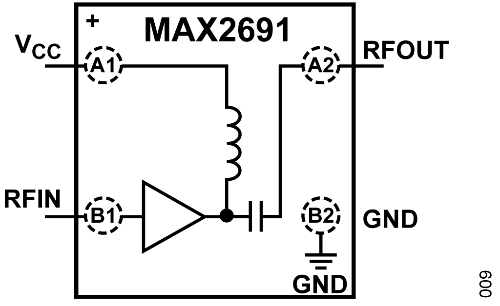
MAX part numbers with four or five digits (for example MAX2657 and MAX12000) are an older family of devices mostly developed for specific applications such as automotive FM radio, global positioning system (GPS), and global navigation satellite systems (GNSS) receivers. These silicon based devices are all internally matched and operate from a single positive supply voltage (see example in Figure 9).

The HMC-ALHXXX-DIE family (for example HMC-ALH216-DIE) are older devices, which are only offered in die form, that feature a frequency coverage from 500MHz to 86GHz (see example in Figure 10). These devices are internally matched and require a negative gate biasing voltage.


LNAs with three digit part numbers (for example HMC311ST89) along with the HMC1XXX and ADL55XX belong to a large older family of general purpose devices (see example in Figure 11). The majority but not all of these devices are internally matched. Moreover, the majority of these devices require a negative gate voltage with the remainder running from a single positive supply with a fixed bias.


Approximately 70 parts from Analog Devices family of 200 LNAs are in die form factor. These devices feature the same functionality as the packaged versions of the parts, but these parts are not in an integrated circuit (IC) package. LNAs in die form tend to have a slightly higher gain and bandwidth, and a lower noise figure than the equivalent packaged version. The nomenclature on LNAs in die form is fairly inconsistent. For example, ADL8106CHIPS, HMC1040-DIE, and HMC1127 are all part numbers for LNAs in die form. To find and differentiate all suitable parts, use the Analog Devices parametric search tool and sort via the package option.
Device Selection Based on Age and Production Status
When selecting an LNA, it is worthwhile to check the age of the device and its production status. This information can be found on the device product page or in the parametric search table. The launch date indicates when the device went into mass production. It is generally recommended to select the newest device that meets your technical needs. Table 2 lists the various production status indicators and its meaning.
| Production Status | Interpretation |
| Recommended for new designs | This product has been released to the market. For new designs, Analog Devices recommends the usage of these products. |
| Production | At least one model within this product family is in production and available for purchase. The product is appropriate for new designs but newer alternatives may exist. |
| Not recommend for new designs | This designates products that Analog Devices does not recommend broadly for new designs. |
| Last time buy | This device is going out of production and this is an opportunity to stock up if device is still currently utilized. |
| Obsolete | The models in this product family are no longer available. The product page for the device may suggest a substitute. |
What Is the Difference Between LNAs, Gain Blocks, and Driver Amplifiers?
The terms LNA, gain block, and driver amplifier are used widely in the industry but are not well defined. There is no agreed upon definition for what constitutes an LNA, that is, there is no threshold for the device noise figure to be below a certain level before it can be called an LNA.
Gain blocks are generally understood to be relatively low power RF amplifiers, which are internally matched and exhibit a relatively wide operating frequency range (for example at least five octaves).
However, a number of LNAs from Analog Devices meet this criteria. Driver amplifiers are generally used to drive ADCs or RF power amplifiers. In both cases, the output specifications such as third order intercept (OIP3), second order intercept (OIP2), and compression (OP1dB) are critical to the end application. However, based on Analog Devices LNA portfolio, a number of devices feature an excellent output referred specifications and can, therefore, be used as driver amplifiers. This suggests that when looking for a device, focus more on the target specifications rather than what the device is defined as. These specifications are discussed further in next sections.
What Are the Criteria for Selecting a Low Noise Amplifier?
Frequency Range
The specified frequency range for an LNA is the range over which Analog Devices has judged the device to work well. This specified frequency range is primarily determined by the behavior of gain, noise figure, and return loss of the device versus frequency. The degradation of these characteristics outside of the specified frequency range is generally graceful. Also, a number of data sheets and s-parameter data sets include data that goes beyond the specified frequency range. This allows the end user to judge and decide whether to use the device outside of the specified range. Figure 12 shows the gain and return loss versus frequency for the HMC8413, a 10kHz to 10GHz LNA. The plot is scaled to 12GHz so that the behavior above 10GHz is apparent.
Due to the internal broadband matching on most devices, it is generally not possible to extend the frequency range of devices through the use of external matching circuitry. For broadband devices that require an external drain biasing inductor (such as the HMC8413), the choice of an inductor can reduce the operating frequency range. The AN-2061: Application Note, Wideband Bias Tee Design Using 0402, SMD Components details more on this topic. It presents a surface-mount bias tee circuit that has a flat response beyond 20GHz for broadband amplifiers that require external bias inductors (a bias tee is a circuit used to provide DC bias current and AC coupling; it consists of a series capacitor and a shunt inductor that is usually connected to the positive power supply).


Gain
LNAs typically have a fixed gain. If a precise gain is required, the most practical way to achieve this is to choose an amplifier with a gain that is slightly higher than necessary and then add attenuation to the circuit. This can be achieved using a T attenuator (a resistor based attenuator that consists of a series resistor and a shunt resistor followed by another series resistor) or a Pi attenuator (a resistor based attenuator that consists of a shunt resistor and a series resistor followed by another shunt resistor) at the input and/or output of the amplifier or by including a digital step attenuator (DSA) in the signal chain. If the LNA is at or close to the start of the signal chain where its noise figure has a large impact, any gain reducing attenuation must be placed after the LNA.
Adjusting the bias current has a slight impact on the gain, but should not, in general, be used as a gain control mechanism. It generally requires significant movement of the bias current to affect a relatively small change in gain. This bias current adjustment tends to have a larger impact on compression and distortion.
IDQ and IDD
Recent Analog Devices LNA data sheets make a distinction between quiescent and dynamic current consumption. Quiescent current (IDQ) is the current consumption when the amplifier is biased on but no RF signal is present. Dynamic current consumption (IDD) is the current consumption when an RF signal is present. IDD is usually but not always higher than IDQ. When dimensioning power management systems, it is important to budget for enough current to support the highest expected RF output power. This includes active bias control circuits where the continuous bias current must be set to support maximum expected output power. Figure 13 shows current consumption, gain, output power, and power added efficiency (PAE) versus input power for the ADL8107, a 6GHz to 18GHz LNA. In this case, IDQ is 90mA and IDD maxes out at 123mA when the input and output power are at +5dBm and +20dBm respectively. Note, that the behavior of IDD versus output power tends to change with signal frequency.


Noise Figure
After frequency range, the noise figure of an LNA is among the most critical specifications. A data sheet publishes a typical noise figure on its font page with specifications at various spot frequencies in the specification tables and plots of noise figure versus frequency and other variables in the typical performance characteristics section of the data sheet.
As frequency increases, noise figure tends to degrade steadily. As frequency decreases, noise figure tends to improve gradually before rising steeply at a certain break point that is usually in the tens or hundreds of MHz. Since most LNAs from Analog Devices are internally matched, this performance cannot be improved using external matching circuitry.
For devices that have an adjustable supply voltage range (for example 3V or 5V), adjusting the supply voltage may impact the noise figure. Moreover, adjusting the bias current might or might not have an impact on noise figure. Figure 14 shows a typical plot of noise figure versus frequency and bias current. In this case, the noise figure of ADL8140, a 10GHz to 18GHz LNA, improves by about 0.3dB as the bias current is increased from 20mA to 45mA. Changing the supply voltage of this device from 1.2V to 3.5V while keeping the bias current at 35mA results in only a 0.1dB improvement in noise figure. However, there are other devices where adjustments on supply voltage or bias current have no noticeable impact on noise figure. Thus, it is best to consult the data sheet of the device you are considering to use to see how the device behaves.


Residual Phase Noise
Residual phase noise is a measure of how much phase noise is added by the amplifier. It is a critical specification for amplifiers that are being used as local oscillator buffers or in radar receivers because the amplifier can add phase noise to the system and, thereby, desensitize it. Residual phase noise is measured by observing the phase noise at the output of the amplifier and canceling out the phase noise of the input signal driving the amplifier. Residual phase noise tends to vary with the RF output power level of the amplifier. It often improves when the output power is at compression or saturation compared to when the amplifier is operating well backed from compression. However, this behavior is not universal.
Residual phase noise is typically presented in data sheets for newer devices in plots at multiple frequencies at PSAT, OP1dB (output 1dB compression point in dBm), and with the output power backed off approximately 10dB from compression. An example plot is shown in Figure 15. In this case, the phase noise improves as the output power increases. However at saturation, the phase noise degrades slightly at some frequency offsets compared to the phase noise at compression. Note that the apparent phase noise increase above 1MHz offset frequency is most likely a measurement artifact caused by imperfect cancellation of the source phase noise in the setup.


Second and Third Order Intermodulation
The second and third order intercept points, which are commonly referred to as OIP2 (output second order intercept point in dBm) and OIP3 (output third order intercept point in dBm), are indicators of the second order (F1 + F2, F1 − F2) and third order (2F1 − F2, 2F2 − F1) intermodulation products that the device produces. For LNAs from Analog Devices, OIP2 and OIP3 are generally measured using a 1MHz separation between the two input carriers at a power level that is typically 10dB to 20dB below the 1dB compression point. This level is specified in the specification table, and some data sheets provide IP3 and IMD3 data (in dBm and dBc) at different power levels.
Second and Third Harmonic
In wideband applications or applications where the LNA is driving an ADC, the size of the second and third harmonic might be important. Some Analog Devices data sheets contain plots of second and third harmonic versus frequency, but most do not. Where harmonic data is not available, the second and third order intermodulation specifications can be used to estimate the magnitude of the second and third harmonics using the following equations:


Where:
PO is the power of the fundamental in dBm.
OIP2 and OIP3 are the second and third order intercept points in dBm.
Note that HD2 refers to second harmonic in dBc while HD3 refers to third harmonic in dBc.
Compression and Saturation
As you increase the RF input power to an RF amplifier, the output power rises proportionally until it starts to compress. The 1dB compression point is the point when the RF output power level and gain are 1dB lower than they should be. Analog Devices generally specifies output referred 1dB compression or OP1dB. Output referred compression is related to input referred compression (IP1dB) by the following equation:

The output saturation point (PSAT) is reached when the RF output power no longer responds to increased input power. For GaAs and silicon devices, PSAT is typically 1dB to 3dB higher than the compression point (for GaN devices the delta between OP1dB and PSAT tends to be larger).
For LNAs whose power supply voltage can be varied (for example, if the LNA supports 3.3V and 5V operation), OP1dB and PSAT is generally higher at higher supply voltages. For devices that have an adjustable bias current (either via a negative gate voltage or an RBIAS resistor), OP1dB can be significantly impacted by the bias setting with higher bias currents generally resulting in a higher OPIdB. An example of this is shown in Figure 16.


While higher supply voltage tends to increase PSAT, the relationship between PSAT and bias current varies by device. In some cases, increasing the current also increases the PSAT but the PSAT levels of the other devices are less responsive to increased bias currents. An example of this shown in Figure 17.


Overdrive Recovery
Overdrive recovery is a measure of how quickly an amplifier returns to its normal operation after it has been driven deep into saturation. In this case, the RF input power is high enough to drive the amplifier into saturation while not exceeding the absolute maximum rating specifications for an RF input power. Overdrive recovery is measured by alternating the input level between a high power signal (often called the blocking signal) that puts the amplifier into saturation followed by a lower level signal (usually at a different frequency) that brings the amplifier back to linear operation. The time it takes for the output to switch from deep saturation back to linear operation is then measured.
When the blocking signal is present, the measured input to output gain is significantly reduced. Once the blocking signal is removed, the input to output gain eventually returns to its specified small signal level. Overdrive recovery is usually defined as the time from removal of the blocker to the gain returning to 90% of its small signal value.
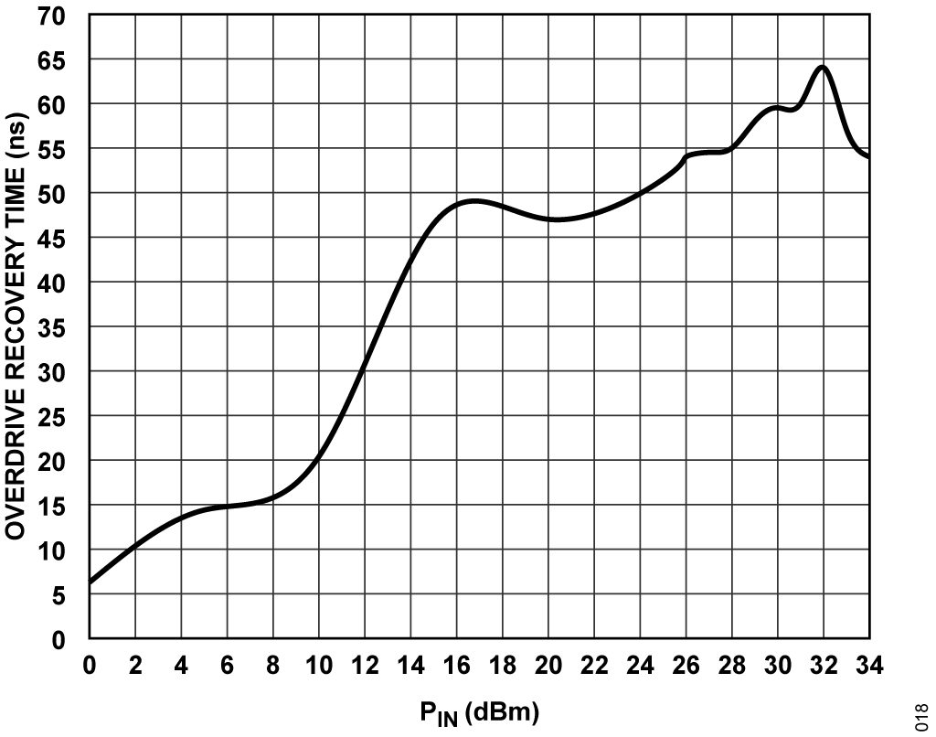
Overdrive recovery times tend to vary as a function of the level of the blocking signal. As a result, the data sheet usually provides a plot of overdrive recovery time versus blocking level instead of a specification in the specification table (see Figure 18 for an example). A data sheet typically includes one overdrive recovery plot, which is taken at one frequency. For wideband devices, the overdrive recovery behavior does not change markedly versus frequency, power supply level, or bias current setting.

Enable/Disable Response Time
In some power sensitive applications, it is necessary to disable the LNA when it is not in use. Some newer LNAs, such as the ADL8108, include a digital input pin, which can be used to power up and power down the device in 15ns and 10ns respectively. Where this function is not available, the RBIAS pin can be used as an enable/disable function. However, the enable/disable response can vary because of the device architecture. This is described in further detail in AN-2599: Application Note, Using the RBIAS Pin of Single Positive Supply RF Amplifiers as a Fast Enable/Disable Input.
Input Survivability and Maximum RF Input Power
While noise figure and input sensitivity are the most critical specifications of an RF receiver, input survivability is also important, particularly in applications such as radar and electronic warfare where deliberate jamming using high powered signals is common. The input survivability of an LNA is specified in dBm in the absolute maximum ratings section of the data sheet. LNAs that can survive relatively high input power levels are specifically referred to as devices with high input survivability in its product descriptors.
The input survivability of the LNA, when the RF input signal is pulsed, tends to be slightly higher (typically 1dB to 3dB). Survivability versus pulsed input power is generally not specified in the device data sheet. If it is specified, this information is provided in the absolute maximum ratings section.
Electrostatic Discharge (ESD) Rating
Information about the ESD susceptibility of the LNA is found in the absolute maximum ratings section of the data sheet. Most data sheets only provide a human body model (HBM) specification. Table 3 summarizes the voltage ratings for the various HBM ESD ratings. If a device is rated Class 1A for example, this means that it survived a 250V HBM pulse and was damaged by a 500V pulse. If no ESD rating is included in the data sheet, assume that the rating is Class 0.
| HBM ESD Class | Voltage Range |
| Class 0 | 0V to <250V |
| Class 1A | 250V to <500V |
| Class 1B | 500V to <1,000V |
| Class 1C | 1,000V to <2,000V |
| Class 2 | 2,000V to <4,000V |
| Class 3A | 4,000V to <8,000V |
| Class 3B | ≥ 8,000 volts |
Thermal Resistance
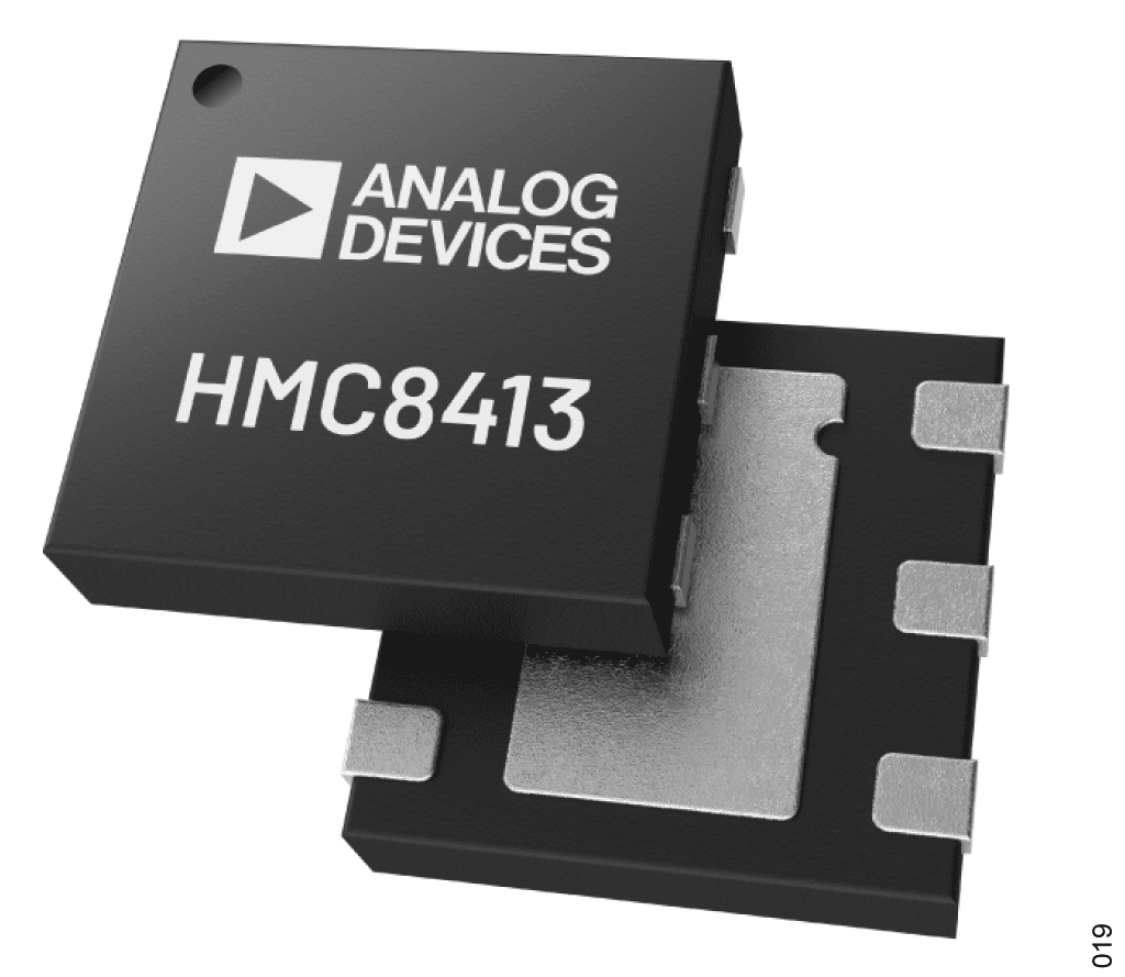
Thermal resistance of an integrated circuit is a measure of how easily heat generated in the die dissipates into the outside world. In the case of most newer LNAs, the die sits on a metal slug, which is exposed on the underside of the device (see Figure 19). As a result, the primary heat flow path is from the die to the metal slug to the printed circuit board (PCB). This assumes that the metal slug of the device makes good thermal contact with a metal pad on the top layer of the PCB, which has an onward heat conduction path (for example, vias which go through the board and connect to a heat sink). In this scenario, there is very little heat conduction from die to air, that is, through the top of the package or from the die to the pins. As a result, most RF amplifier data sheets just specify junction to case thermal impedance.

A high junction-to-case thermal resistance is not necessarily problematic. The ultimate goal of thermal resistance calculations is to establish that the die is not exceeding its specified maximum junction temperature (usually 175°C for GaAs amplifiers). The equation for calculating the junction temperature is as follows:

For example, if θJC is 100°C/W and power dissipation is 100mW, the junction temperature is 95°C if the case is at its maximum temperature of 85°C. In this case, the device has a high thermal resistance but the junction temperature is at a safe level because the power consumption is relatively low. This topic is discussed further in AN-2591: Application Note, When It Comes to Long-Term Reliablity of RF Amplifier ICs, Focus First on Die Junction Temperature.
As most heat flow is through the bottom of the package and into the PCB, any heat sinking is generally implemented on the underside of the PCB. A heat sink can be added to the top side of the package, but it is generally of little benefit because the junction-to-case top thermal resistance is much higher than the junction-to-case bottom thermal resistance (θJC).
Power Supply Requirements and Sequencing
LNAs developed on depletion mode and enhancement mode process differ in the key respect that the depletion mode devices require a negative gate voltage and the enhancement mode devices do not. As this has a significant impact on the power supply design, it must be taken into consideration when choosing a device.
Figure 20 shows a typical power management circuit for an enhancement mode LNA. In this example, the LT8607 step-down regulator is used to step down a 12V rail to 5.5V, which is then applied to the LT3042 low dropout (LDO) linear regulator, which generates a low noise 5V output and suppresses the switching spurs from the buck regulator. The LT8607 can accept input voltages as high as 42V and can source up to 750mA. The LT3042 low dropout regulator can source up to 200mA. If power supply voltage is being developed as a bus supply to serve multiple components, higher current devices can be used. The LT8608 and LT8609 step-down regulators can source maximum currents of 1.5A and 3A respectively. These devices are pin compatible with the LT8607. The LT3045 linear regulator, which is pin compatible with LT3042, can source up to 500mA.

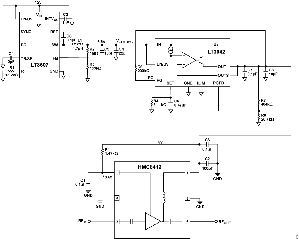
Figure 21 shows an application circuit for the ADL8106, an 18GHz to 54GHz LNA. In this circuit, the HMC920 active bias controller is being used to generate the positive supply voltage (VDD) and the negative gate voltage (VGG). The active bias controller safely sequences these two voltages and uses negative feedback to adjust the gate voltage until the desired set point drain current is flowing. This current is set by a resistor connected to the HMC920 (R4 in the schematic), and must be set high enough to provide the highest expected drain current for the application, which always flows (140mA in this case). HMC920 can operate from supply voltages from 5V to 16.5V. It can generate drain voltages from 3V to 15V. The available gate voltage range is 0V to –2.5V, and the drain current can be set between 0mA and 500mA.


As an alternative to an active bias control circuit, a fixed negative voltage generator can also be used, such as the ADP5600 along with a positive LDO. However, for a number of reasons, this is not recommended. Fixing the gate voltage means that you are subject to part variations in the drain current. The relationship between drain current and specifications, such as compression and distortion, is tighter than their relationship to the gate voltage. If the same gate voltage is applied to multiple devices, each one has a slightly different drain current. More of this is discussed in AN-1363: Application Note, Meeting Biasing Requirements of Externally Biased RF/Microwave Amplifiers with Active Bias Controllers. Thus, it is better for multiple devices to have the same drain current versus the same gate voltage. Moreover, you need to be careful with the sequencing. Make sure to use the power good (PG) output from the negative gate voltage generator to gate and enable the positive supply. This ensures that the gate voltage is present before the drain voltage.
External Component Count
In addition to the required power management circuitry, the number of external passive components that the LNA requires is an important consideration. External AC coupling capacitors and bias inductors may be required or may be integrated. In general, the more octaves covered by the device, the higher the likelihood that external AC coupling capacitors and a biasing inductor are required. For example, the HMC8412 operates from 400MHz to 11GHz and integrates its AC coupling capacitors and bias inductor, while the ADL8101 operates from 10KHz to 22GHz, but requires two external capacitors and a bias inductor. Design of wideband external biasing networks is covered in detail in AN-2061: Application Note, Wideband Bias Tee Design Using 0402 SMT Components. Where operation to frequencies in the KHz range is required, physically larger components are required.
The requirement for external matching components must also be considered when selecting an LNA. The majority of LNAs from Analog Devices are internally matched, but some devices do require external matching components for stability or to improve the input and/or output return loss.
A commonly asked question is whether the device can operate with less power supply decoupling capacitors are specified in the data sheet. The power supply and gate voltage decoupling capacitors shown in the basic connections circuit in the data sheet represent the configuration used to characterize and qualify the device. If you want to reduce the number of capacitors, it is recommend to first remove or combine the largest capacitors that are farthest from the device and verify that there is no impact on noise or stability.
In general, every VDD and VGG pin should have at least one capacitor.
Availability of Simulation Models
Analog Devices provides s-parameters for all of its LNAs on the device product page. For the latest devices, s-parameter data is provided at multiple temperatures. Unless otherwise stated in the s-parameter header file, s-parameters are measured from the input connector to output connector of the evaluation board with a scalar correction of the gain/S21 to compensate for input and output trace losses. Figure 22 shows a portion of the s-parameter data set for the ADL8102, a 1GHz to 22GHz LNA.


Analog Devices also provides sys-parameter models for use in Keysight Genesys and SystemVue. These models include s-parameter data along with noise figure, compression, OIP2, OIP3, and PSAT. Figure 23 shows a portion of the sys-parameter data set for the ADL8102. The most recent library of sys-parameter models can be downloaded at www.analog.com/sys-parameters. For the latest devices, the s-parameter zip file also contains a .CSV file that includes noise and distortion data. This file can be used to build nonlinear models in other simulation platforms. AN-2560: Application Note, Creating Amplifier2 Models in Keysight ADS Using Genesys and SystemVue Sys-Parameter Models describes the steps required to convert a sys-parameter model into an AMP2 nonlinear model, which can be used in Keysight advanced design system (ADS).


Similar to data sheet plots, s-parameter and sys-parameter data sets often provide data that goes beyond the specified frequency range of the device.
Is There a Checklist for Selecting an LNA?
Use the following checklist as a step by step guide to define your requirements and narrow down your options so that you select the device that best meets your needs.
-
Determine the primary specifications of the end application by the following
parameters:
- Gain
- Frequency range
- Noise figure
- OIP3 and OIP2
- Supply voltage and current consumption
- Determine if the application requires a die or a packaged part.
- Use the product selection tool on Analog Devices website to narrow down the choices to four or five devices. Try to choose devices that are listed as production or recommended for new designs. Avoid selecting not recommended for new designs or last time buy.
-
Determine the value of secondary specifications from the device data sheets:
- RF input power survivability
- Overdrive recovery time
- Residual phase noise
- ESD rating
- If you plan to perform simulations, download the s-parameters from the device product page. For Keysight Genesys and SystemVue users, the most recent sys-parameter library can be downloaded at www.analog.com/sys-parameters.
- Finalize your device selection.
Conclusions
Analog Devices has an extensive portfolio of LNAs. To narrow down your options, focus on the latest devices that operate from a single positive supply (with production status that is equal to recommended for new designs or tagged as in production). These devices are simple to operate and only require a few external passive components to operate. If you choose an LNA that requires a negative gate voltage, biasing and safe sequencing can be provided by the HMC920.
References
Soc, Ivan. Nash, Eamon. AN-2061: Wideband Bias Tee Design Using 0402, SMD Components. Analog Devices, 2024.
Soc, Ivan. Nash, Eamon. AN-2591: When It Comes to Long-Term Reliability of RF Amplifier ICs, Focus First on Die Junction Temperature. Analog Devices, 2024.
Bedrosian, Jim. Nash, Eamon. AN-2560: Creating Amplifier2 Models in Keysight ADS Using Genesys and SystemVue Sys-Parameter Models. Analog Devices, 2023.
Kaya, Kagan. AN-1363: Meeting Biasing Requirements of Externally Biased RF/Microwave Amplifiers with Active Bias Controllers. Analog Devices, 2022.
Smith, Dorant. AN-2599: Using the RBIAS Pin of Single Positive Supply RF Amplifiers as a Fast Enable/Disable Input. Analog Devices, 2024.
Appendix: Frequently Asked Questions
- What is an RF low noise amplifier (LNA)?
An RF LNA is a front-end amplifier designed to boost signal levels while introducing minimal noise, thereby improving overall receiver sensitivity. There is no universally accepted threshold for the noise figure below which an amplifier qualifies as a low noise amplifier. In addition to low noise, many LNAs incorporate features such as high input survivability, high input linearity, and a bypass mode, making them well suited for deployment at the often hostile front end of an RF receiver.
- Why is noise figure the most important LNA parameter?
The noise figure determines how much noise the LNA adds to the signal and directly limits receiver sensitivity, especially since the noise figure of the first stage dominates the cascaded performance.
- What is the difference between an LNA and a gain block?
There is no strict definition; LNAs are typically optimized for low noise, while gain blocks emphasize broadband operation and moderate noise and linearity. It is better to select an LNA be based on specifications rather than device classification.
- Can an LNA be used as a driver amplifier?
Like gain blocks, there is not a strict definition of the term driver amplifier. It is generally understood to be a component that is used toward the end of a signal chain (for example, driving an analog-to-digital converter (ADC) in a receiver or driving a power amplifier in a transmitter). Because driver amplifiers typically handle relatively high-level signals, distortion and compression become critical considerations and noise figure may become less important. Many LNAs have relatively low distortion and high output compression (since they have to deal with blockers), which means they often have sufficient performance to be used as driver amplifiers.
- Can I use an LNA beyond its specified frequency range?
The specified frequency range defines where gain, noise figure, and return loss meet data sheet expectations. Analog Devices data sheets and s-parameter files often provide performance plots that go beyond the specified frequency range. This is provided for informational purposes, allowing engineers to decide whether the out-of-range performance is acceptable in their application.
- Can external matching extend the frequency range of an LNA?
For most internally matched LNAs, external matching does not significantly extend bandwidth; performance is largely defined by the internal design.
- Can gain be adjusted by adjusting the bias current of the amplifier?
Bias current changes typically produce only small gain variations and are better used to control linearity and compression performance. For example, if you adjust the bias current to reduce gain by 0.5dB, you may find that IP3, IP2, and P1dB suffer a more significant reduction. Analog Devices data sheets typically provide performance plots showing the effects of bias current changes on gain, noise, linearity, and return loss.
- What is OIP3 and why is it important?
Output third-order intercept (OIP3) indicates how much intermodulation distortion the LNA produces and is critical for systems where strong interfering signals are present For example consider the case where there are two blockers present at 2.001GHz and 2.002GHz respectively and that the receiver is trying to tune to a signal at 2GHz, The two blockers will intermodulate and produce and third order intermodulation (IMD3) products at 2GHz and at 2.003GHz . If the IMD3 product at 2GHz is large enough, the receiver will not be able to tune to the wanted signal.
- What is OP1dB?
Output 1‑dB compression point (OP1dB) is the output power level at which the amplifier’s gain drops by 1dB compared to its small-signal gain (that is, S21 from S-parameters). It is commonly used to set a safe operating level in applications that require good linearity. A typical guideline is to operate with some margin below compression (for example, operate at OP1dB minus 10dB).
- What is the difference between OP1dB and PSAT?
OP1dB marks the onset of compression, while PSAT represents the maximum output power at which further increases in input no longer produce higher output. For GaAs LNAs, the delta between OP1dB and PSAT is typically 1dB to 3dB.
- How does supply voltage affect OP1dB, IP3, IP2, PSAT, noise figure, and gain?
A higher supply voltage typically increases OP1dB, PSAT, OIP2, and OIP3 (this varies by device, so it is important to consult device data sheets). It is difficult to make general statements about the effect of supply voltage on the noise figure and gain of an LNA. So it is necessary to consult the data sheet.
- How does drain/bias current affect OP1dB, IP3, PSAT, and gain?
Higher bias current typically increases OP1dB and OIP3 but tends to have less impact on PSAT, gain, and noise figure (this varies by device, so it is important to consult device data sheets).
- Why do I need to budget for IDD and not just IDQ?
IDD is the current drawn under RF drive and will usually exceed IDQ, the quiescent current with no RF present. From the data sheet RF power sweep plots, you can determine the maximum IDD based on the maximum expected RF output level. Once this is known, the power management system for the LNA must be dimensioned to support this current. It is important to note that if you are using an active bias controller, the setpoint current must be configured to this maximum level.
- When does overdrive recovery matter?
In pulsed or jammer-rich environments, deep compression can occur; recovery time determines how quickly the receiver can return to linear operation after the jammer signal has subsided. In a RADAR for example, fast overdrive recovery will reduce the time that the RADAR is blind after the jammer is removed.
- If no ESD rating is listed, what must I assume?
In particular for HMC LNAs where there is no ESD rating in the data sheet, assume that the device is Class 0.
- When turning on a depletion mode LNA, Analog Devices data sheets recommend first setting the gate voltage (VGG1) to pinch-off, then applying the drain voltage (VDD), and finally increasing the gate voltage (moving it more positive, toward 0V) until the desired current flows. Is there an easier way to turn on the LNA in a safe manner?
If you know the final VGG1 gate voltage you plan to apply, you can skip the pinch-off step, that is, start by applying the final VGG1 gate voltage (for an LNA with a pinch-off voltage of −2V, this voltage might be something like −1V) before applying the VDD drain voltage.
- Is there a way to quickly turn LNAs on and off?
Some newer LNAs, such as the ADL8108, a 1GHz to 8GHz LNA, include a digital input pin that can be used to quickly power the device up or down with typical response times are in the 10ns to 15ns range. This pin is usually called VPD or VENBL. Where this function is not available, the RBIAS pin can be used as an enable/disable function. This is described in further detail in AN-2599 Application Note, Using the RBIAS Pin of Single Positive Supply RF Amplifiers as a Fast Enable/Disable Input. Depletion mode LNA which have a negative gate voltage can be disabled by setting the gate voltage to its pinch-off value which is usually in the −1.5V to −2V range.
- Are there instances where external AC-coupling capacitors are required on RFIN and RFOUT even when the part has internal AC-coupling capacitors?
If there is a DC path to ground on the pin-side of an internal AC-coupling capacitor, you need to AC-couple your input or output signal if it is not sitting at a DC bias level of 0V. Check the device block diagram or the interface schematics section of the data sheet for this information. Take a look for example at the block diagram and interface schematics for ADL8142, a 23GHz to 31GHz LNA. If this device is driving a subsequent stage which has a non-zero bias voltage level, an external AC-coupling capacitor would be required at the output because of the internal inductor to ground at RFOUT.
- Why is it that most Analog Devices LNA data sheets do not specify junction-to-air thermal impedance?
In most newer LNAs, the die is mounted on a metal slug that is exposed on the underside of the package. As a result, the primary heat flow path is from the die to the metal slug to the printed circuit board (PCB). This results in very little heat conduction from die to air, that is, into the air through the top of the package. In this scenario, the junction-to-air thermal resistance number is of little value, since adding top-side heat sinking will not significantly affect the junction temperature.
Author
