Reverse Voltage Protection for Battery Chargers
Introduction
There are some well known techniques for handling source voltage reversal. The most obvious is a diode from the source to the load, but it has the downside of extra power dissipation due to the diode forward voltage. As elegant as it is, a diode will not work in portable or backup applications since the battery must sink current when charging and source current when not.
Another approach is to use one of the MOSFET circuits shown in Figure 1.

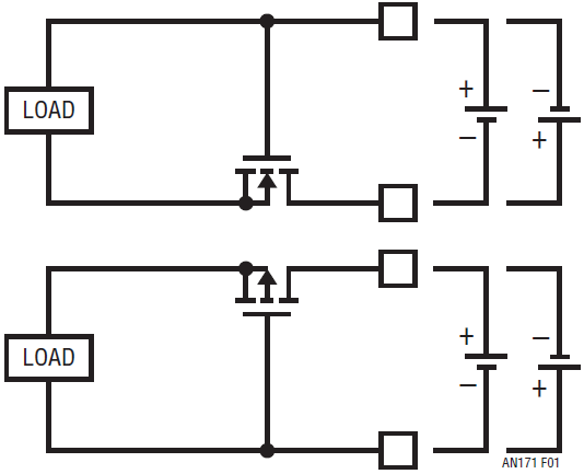
For load side circuits, this approach is superior to the diode since the source (battery) voltage enhances the MOSFET, yielding less voltage drop and effectively higher conductance. The NMOS version of the circuit is preferable over the PMOS version due to the higher conductivity, lower cost and better availability of discrete NMOS transistors. In both circuits, the MOSFET conducts when the battery voltage is positive and disconnects when the battery voltage is reversed. The physical “drain” of the MOSFET becomes the electrical source since it is the higher potential in the PMOS version and the lower potential in the NMOS version. Since MOSFETs are electrically symmetrical in the triode region, they will conduct current in both directions equally well. With this approach, the transistor must have a maximum VGS and VDS rating greater than the battery voltage.
Unfortunately, this approach is only valid for load side circuits and will not work with a circuit that can charge the battery. The battery charger will produce power, reenabling the MOSFET and reestablishing the connection to a reversed battery. An example using the NMOS version is shown in Figure 2 where the battery is shown in the fault state.

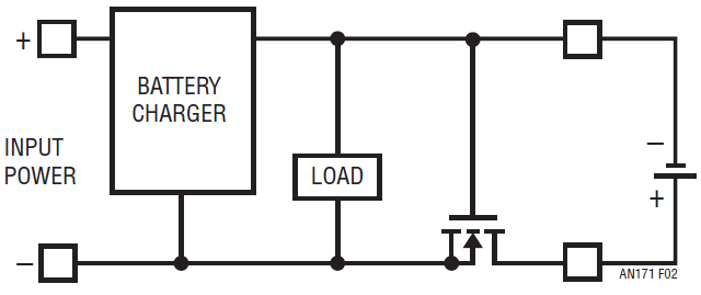
When the battery is connected, and the battery charger is inactive, the load and battery charger are safely decoupled from the reversed battery. However, if the charger becomes active, for instance if the input power connector is attached, then the charger produces a voltage from the gate to the source of the NMOS, enhancing it, resulting in conduction. This can be visualized better in Figure 3.

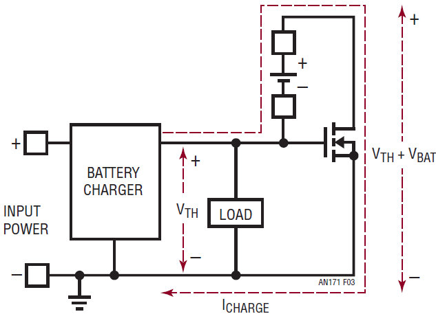
The load and charger are isolated from the reverse voltage but the protection MOSFET now suffers exceedingly high power dissipation. In this scenario, the battery charger becomes a battery discharger. The circuit will come to equilibrium when the battery charger produces enough gate support for the MOSFET to sink the current delivered by the charger. For instance, if the VTH of a strong MOSFET is around 2V, and the charger can deliver current at 2V, then the battery charger output voltage will settle at 2V with the drain of the MOSFET at 2V plus the battery voltage. The power dissipation in the MOSFET is ICHARGE • (VTH + VBAT), heating the MOSFET until it flows off the printed circuit board. The PMOS version of this circuit suffers the same fate.
Two alternatives to this approach are presented below, each having advantages and disadvantages.
N-Channel MOSFET Design
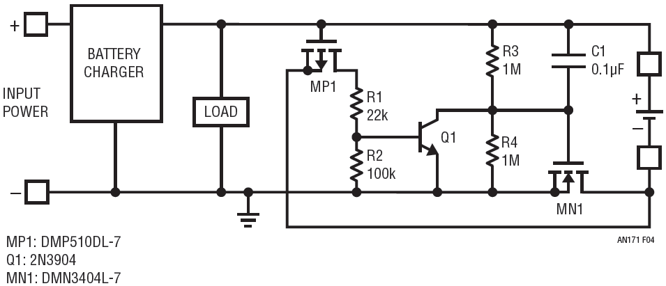
The first approach uses an NMOS blocking device as shown in Figure 4.
The algorithm for this circuit is that the blocking MOSFET must be disabled if the battery voltage exceeds the battery charger output voltage.
In this circuit MN1 is connected in the low side of the connection between the charger/load and the battery terminals as in the NMOS approach described above. However, transistors MP1 and Q1 now provide a detection circuit that disables MN1 if the battery is reversed. A reverse connected battery will lift the source of MP1 above its gate, which is connected to the charger’s positive terminal. The drain of MP1 then, in turn, delivers current to the base of Q1 through R1. Q1 then shunts the gate of MN1 to ground, preventing the charge current from flowing in MN1. R1 controls the base current to Q1 during reverse detection and R2 provides a bleed for the base of Q1 in normal operation. R3 gives Q1 the authority to pull MN1’s gate to ground. The R3/R4 voltage divider limits the voltage on MN1’s gate so that the gate voltage doesn’t have to plunge as far during a reverse battery hot plug. The worst case is when the battery charger is already active, producing its constant-voltage level, when a reversed battery is attached. In this case MN1 needs to be turned off as fast as possible to limit the time in which high power is being dissipated. This particular version of the circuit with R3 and R4 is best suited for 12V lead-acid applications but R4 could be eliminated in lower voltage applications such as 1 and 2 cell Li-Ion products. Capacitor C1 provides an ultra-fast charge pump to drive the gate of MN1 down during reverse battery attach. C1 is particularly helpful for the worst-case scenario where, again, the charger is already enabled when a reverse battery attach occurs.
This circuit has the disadvantage of requiring extra components and that the R3/R4 divider creates a small, but continuous, load on the battery.
Most of these components are tiny. MP1 and Q1 are not power devices and can usually be found in small packages like a SOT23-3, an SC70-3 or even smaller. MN1 should be very conductive, since it is the pass device, but does not need to be physically large. Since it operates in deep triode with large gate enhancement, its power dissipation will be low even for a moderate conductivity device. For instance, sub 100mΩ transistors can often be found in a SOT23-3 as well.

The down side of a small pass transistor, however, is that extra impedance in series with the battery charger extends charge time during the constant-voltage charging phase. For instance, if the battery and its cabling have 100mΩ of equivalent series resistance, and a 100mΩ blocking transistor is used, charge time in the constant-voltage charging phase will double.
The detection and disable circuit of MP1 and Q1 are not particularly fast at disabling MN1, and they don’t need to be. Although MN1 sees high power dissipation during reverse battery attach, the turn off circuit just needs to disconnect MN1 “eventually”. It needs to disconnect MN1 before MN1 heats up enough to be damaged. Disconnect time in the tens of micro-seconds is probably fine. On the other hand, disabling MN1 before the reversed battery has a chance to pull the charger and load voltage negative is crucial, thereby requiring C1. Essentially, this circuit has both an AC and a DC disable path.
This circuit was tested with a lead-acid battery and the LTC4015 battery charger. Figure 5 shows the battery charger in the OFF state when the reverse battery hot plug occurs. No reverse voltage is transmitted to the charger and load.

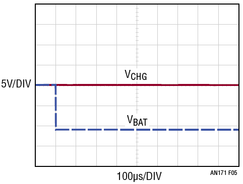
Notice that MN1 needs a VDS rating equal to the battery voltage and a VGS rating of half the battery voltage. MP1 needs a VDS and VGS rating equal to the battery voltage.
Figure 6 shows the more severe case of the charger up and running when the reverse battery hot plug occurs. The reverse connection pulls the charger side voltage down until the detection and protection circuits disengage it, allowing the charger to return safely to its constant-voltage level. Dynamics will vary by application and capacitance on the battery charger will play a large role in the outcome. In this test the battery charger had both a high Q ceramic capacitor as well as a lower Q polymer capacitor

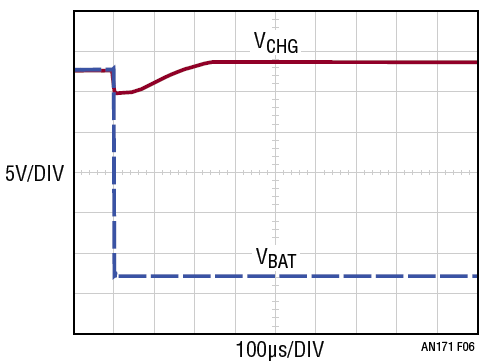
Aluminum-polymer and aluminum-electrolytic capacitors are recommended on the battery charger anyway to improve performance during a normal forward battery hot plug. Due to their extreme nonlinearity, pure ceramic capacitors produce excessively high overshoot during hot plug as their capacitance plunges by a shocking 80% when the voltage increases from 0V to rated voltage. This nonlinearity encourages high current flow at low voltage while rapidly shedding capacitance as the voltage rises; a lethal combination resulting in very high voltage overshoot. Empirically, the combination of a ceramic capacitor and a lower Q, voltage-stable, aluminum or even tantalum capacitor appears to be the most robust combination.
P-Channel MOSFET Design
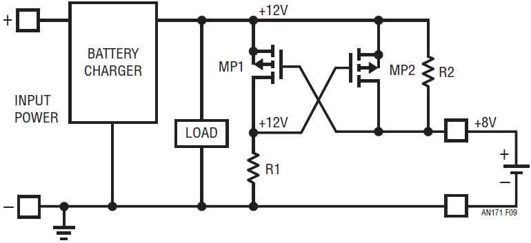
A second approach using a PMOS transistor as the protection device is show in Figure 7.

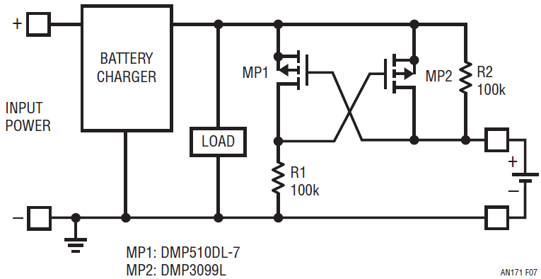
In this circuit, MP1 is the reverse battery detection device and MP2 is the reverse blocking device. The positive battery terminal is compared to the battery charger output by the source to gate voltage of MP1. If the battery charger terminal voltage is above the battery voltage, MP1 disables the primary pass device MP2. Therefore, if the battery voltage is driven below ground, clearly the detection device, MP1, will drive pass device MP2 off by jamming its gate to its source. It will provide this service whether the battery charger is enabled and making charge voltage or disabled at 0V.
This circuit has the supreme advantage that the PMOS blocking transistor, MP2, has no authority to transmit negative voltage to the charger circuit and load whatsoever. Figure 8 illustrates this more clearly.

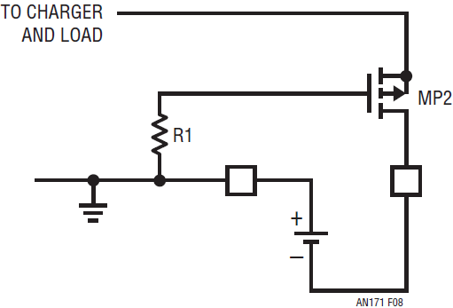
The lowest achievable voltage at the gate of MP2 is 0V via R1. Even if the drain of MP2 is pulled well below ground, its source will not apply significant downward pressure. Once the source voltage gets down to the transistor’s VTH above ground the transistor de-biases itself and its conductance fades. The closer the source gets to ground, the more de-biased the transistor becomes. This characteristic, along with the simple topology, makes this approach more attractive than the NMOS approach shown previously. It does have the disadvantage of the lower conductivity and higher cost of the PMOS transistor versus the NMOS approach.
Although simpler than the NMOS approach, this circuit has another large disadvantage. While it always protects against reverse voltage, it may not always connect the circuit to the battery. With the gates cross-coupled as show, the circuit forms a latching memory element that may pick the wrong state. Although difficult to achieve, a condition exists wherein the charger is producing voltage, say 12V, a battery is attached at a lower voltage, say 8V, and the circuit is disconnected. In this case the source to gate voltage of MP1 is +4V, enhancing MP1 and disabling MP2. This case is shown in Figure 9 with stable voltages listed on the nodes.

To achieve this condition, the charger must have been engaged when the battery was applied. If the battery is applied before the charger is enabled, the gate of MP1 is pulled up by the battery completely disabling MP1. When the charger turns on it produces a controlled current rather than a high-current slug which reduces the chance of MP1 turning on and MP2 turning off.
On the other hand, if the charger is enabled before the battery is attached, the gate of MP1 simply follows the battery charger output as it is pulled up by bleed resistor R2. Without a battery, MP1 has no propensity to turn on and disengage MP2 at all.
The problem occurs when the charger is already up and running and the battery is then attached. In this case there will be an instantaneous difference between the charger output and the battery terminal which will encourage MP1 to disengage MP2 as the battery voltage coerces the charger capacitance to assimilate. This constitutes a race condition between the ability of MP2 to strip charge out of the charger capacitor and the ability of MP1 to disengage MP2.
This circuit was also tested with a lead-acid battery and the LTC4015 battery charger. Connecting a heavily loaded 6V supply as a battery emulator to an already enabled battery charger never triggered the “disconnect” state. Testing was not exhaustive and should be performed more thoroughly in critical applications. Even if the circuit did latch off, disabling the battery charger and re-enabling it will always result in reconnection.
The fault state can be demonstrated by artificially manipulating the circuit with a temporary connection from the top of R1 to the battery charger output. It is believed, however, that this circuit has a significantly higher propensity to connect than to not. If failure to connect does become a problem, it is possible to devise a circuit that will disable the battery charger with more devices. An example is shown in the more complete circuit of Figure 12.
Figure 10 shows the result of the PMOS protection circuit with the charger disabled.

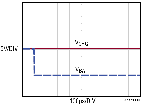
Notice that the battery charger and load voltage show no negative voltage transmission whatsoever.
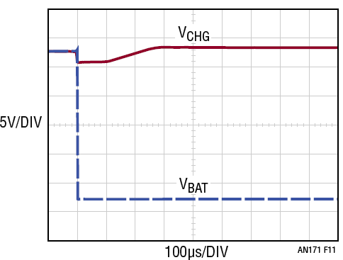
Figure 11 shows this circuit in the sinister condition of the charger already engaged when the reversed battery is hot plugged.
Indistinguishable from the results of the NMOS circuit, the reverse battery pulls the charger and load voltage down somewhat before the disconnect circuit disengages pass transistor MP2.
In this version of the circuit, transistor MP2 must be able to survive a VDS of twice the battery voltage (one for the charger and one for the reversed battery) and a VGS of one battery voltage. MP1, on the other hand, must survive a VDS of one battery voltage and a VGS of twice the battery voltage. This requirement is unfortunate as rated VDS always exceeds rated VGS for MOSFET transistors. It is possible to find transistors with VGS tolerance of 30V and VDS tolerance of 40V which is suitable for lead-acid applications. To support higher voltage batteries, the circuit will have to be modified with extra Zener diodes and current limiting resistors.
Figure 12 shows an example of a circuit that can handle two lead acid batteries stacked in series.


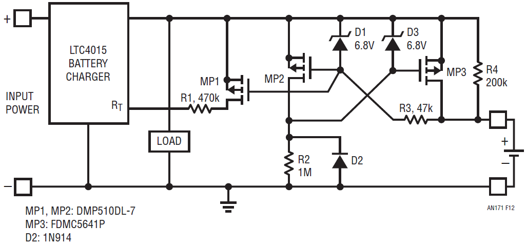
D1, D3 and R3 protect the gates of MP2 and MP3 from high voltage. D2 prevents MP3’s gate from pumping below ground, and the battery charger output with it, when a reversed battery is hot plugged. MP1 and R1 detect when the circuit has either a reversed battery or is in the incorrect disconnect latch state and disables the battery charger by exploiting the missing RT feature of the LTC4015.
Conclusion
It is possible to develop a reverse voltage protection circuit for battery charger based applications. Some circuits were developed and abbreviated testing was performed with encouraging results. There is no silver bullet to the reverse battery problem but hopefully the approaches shown provide sufficient inspiration that a simple, low cost, solution exists.