Circuit Suggestions Using Features and Functionality of New Sigma-Delta ADCs-Part 2

Circuit Suggestions Using Features and Functionality of New Sigma-Delta ADCs-Part 2
著者
John Wynne
2002年06月01日
As a continuation of Part 1, this White Paper explains the features and functionality of new sigma-delta converters from Analog Devices and how they can be used to solve everyday design tasks in a simpler and more cost-effective way than ever before. The explanation of these different tasks is at a relatively high level, but it is hoped that the circuits presented here will fuel your own imagination into producing innovative solutions to your own problems, in your own style.
Part 1 covered these topics:
- Indirect Temperature Measurement of a Bridge Transducer Permits Software Temperature Compensation
- Combining Absolute and Ratiometric Measurement Capability with One ADC
- Minimize Power Dissipation When Measuring Pt100s
- Eliminate Thermoelectric EMFs in Low Resistance Measurements
- For TEC Applications, Implement Your Own Mix of Analog Input and Output Channels
Part 2 covers the following topics:
- Using a Synchronous VFC to Isolate a Smart Actuator
- Measure Differential Temperatures Accurately
- Low Power Touch Screen Application
- Driving a Multi-Axis Sensor for Position Control
- Use New Synchronous VFCs for Low Side Current Sensing
F. Using a Synchronous VFC to Isolate a Smart Actuator
One area where the attributes of high resolution, simple isolation, and the low cost of voltage-to-frequency converters come together is in isolating a smart valve or smart actuator control circuit. Figure F1 shows an AD7740 being used as an isolator while a separate 16-bit sigma-delta ADC, the AD7707, is used to accomplish a number of activities within the locally powered valve. The sense resistor RS (typically 100 Ω to 250 Ω) between VIN and GND converts the twisted-pair loop current into a frequency output that is then transmitted across the opto-isolator to a timer/counter input on the local microcontroller. This loop current, which signals the required valve position to the local microcontroller, can be either 0 mA to 20 mA or 4 mA to 20 mA. For a 0 mA to 20 mA loop as shown in Figure F1, power for the VFC must come from the actuator side. This is the function of the oscillator, transformer T1, components D1 and C1, and low dropout voltage regulator ADP3333. The AD7740 can operate from 3 V to 5 V.
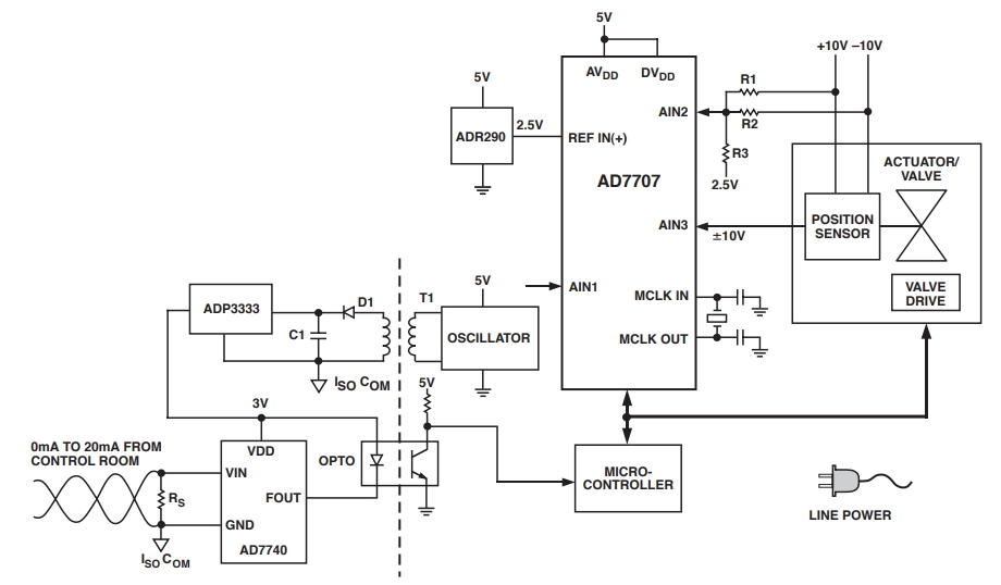
The microcontroller, through one of its timer/counter inputs, accumulates the pulse train from the VFC and ensures that actual and desired valve positions are identical. A valve-position sensor, typically a precision servo potentiometer or an LVDT, monitors the valve position. Due to the noisy environment usually found inside actuators, it is recommended to have as large a signal level as possible. Normally ±10 V would be used as excitation for these position sensors, which in turn leads to a requirement for an ADC that can accept ±10 V inputs directly. The 16-bit AD7707 has three input channels, one of which is a high level input channel capable of accepting true ±10 V input signals directly. The two other input channels are low level channels with input signal ranges of 0 V to ±20 mV through 0 V to ±2.5 V.
In Figure F1, the wiper of the potentiometer is connected to AIN3, the high level input of the AD7707. Due to the input architecture used, the input impedance of this high level channel is finite and resistive with a value of 30 kΩ typically. In choosing the value of potentiometer to use here, it should be noted that large values will cause a linearity error that is dependent on wiper position. For instance, with a 1 kΩ potentiometer, the maximum linearity error is 0.2%. Since the error curve is exactly repeatable, it is possible to reduce this error source to below 0.02% by running a calibration cycle over the full open/close span and retaining the results for re-use by the microcontroller.
The other low level channels can be used for other purposes within the actuator; for instance, they could be used to measure the motor winding temperature with the help of the RTDs attached to the windings. In the diagram, one low level channel is used to monitor the excitation voltages used to power the valve-position sensor. By properly scaling the resistor values R1–R3, appropriately unique signal levels can be produced across R3 that correspond to normal and abnormal operating conditions. Therefore, if either or both of the ±10 V excitation sources fail separately or together, the voltage level on AIN2 will reflect such an occurrence whereas the voltage signal on AIN3 might still be within its allowed limits. Under normal operation with all voltage levels at their correct values, the voltage measured on AIN2 will also be unique and can be readily identified as such by the microcontroller.
G. Measure Differential Temperatures Accurately
Sometimes it is necessary to measure not just the absolute temperature of a single point in a system but also to measure the differential temperature between two other points. These sorts of measurements are found in Thermal Mass flowmeters and in temperature zone controllers in wafer diffusion chambers, among others.
The circuit described here is based on RTDs, but other types of resistive temperature sensors can be used. To ensure the measurements are truly relative, it is necessary to wire all the RTDs in series and excite them with the same current source, IEXC. See Figure G1. The same excitation current also flows through the reference resistor RREF to generate the voltage reference for the ADC so the entire circuit is ratiometric with respect to the excitation. Thus the current source need not be particularly stable over temperature for this circuit to operate. To make an accurate absolute temperature measurement however, the reference resistor has to be a precision one and a precision voltage reference is also needed. Note that differential input pairs AIN1/AIN2, AIN3/AIN4, and AIN5/AIN6 of the AD7708 use the REFIN1(+)/REFIN1(–) differential reference inputs.
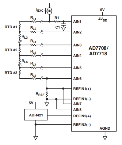
The circuit in Figure G1 shows three RTDs measuring temperature at three sites. The first and third RTD in the string are 3-wire RTDs used to measure the temperature difference between these two sites; the RTD in the middle is a 4-wire RTD and it reports the absolute temperature of its site. If only a temperature difference measurement is required and not an absolute temperature measurement, then this middle RTD can be omitted. The wiring resistances between the local measurement electronics and the RTDs are shown as resistive pairs RL1/RL2, RL4/RL5, and RL7/RL8.
The differential analog input pair AIN1/AIN2 of the AD7708 reads an input voltage equal to:
IEXC(RTD #1) + IEXC(RL1)
where RTD #1 represents the resistance of the first RTD element.
The differential analog input pair AIN5/AIN6 reads an input voltage equal to
IEXC(RTD #3) + IEXC(RL8)
where RTD #3 represents the resistance of the third RTD element.
If the wiring harness for the RTDs is arranged such that RL1 = RL8 then subsequently subtracting the AIN1/AIN2 channel reading from the AIN5/AIN6 channel reading, in software, the ohmic drops cancel out leaving the temperature differential term as the only remaining term. The inter-RTD wiring resistances, labelled RL3 and RL6, do not appear in the equations so the circuit is tolerant of ohmic drops between the RTDs.
Similarly, wiring resistances RL2, RL4, RL5, and RL7 have no effect since no current flows through these wires due to the high impedance input stage of the AD7708. If the AD7708 and related measuring electronics are particularly remote from the RTDs, then noise pickup may be an issue. Since the input impedance of the buffer inside the AD7708 is very high, it is completely acceptable (and recommended) to add external resistor-capacitor combinations on the analog inputs, such as R1 and C1 in Figure G1, to act as low-pass filters to attenuate high frequency noise pickup on the wiring. The reasons for choosing these components is covered in the AD7708 data sheet.
To transfer the ratiometric reading on input pair AIN3/AIN4 to an absolute basis, the final AIN7/AIN8 differential input pair and the second set of differential reference inputs on the AD7708 are used to good advantage. The precision 2.5 V reference, supplied by the ADR421 reference, is applied directly to REFIN2(+)/REFIN2(–), while the differential input AIN7/AIN8 measures the reference voltage used for the RTD measurements. This gives an absolute reading of what the reference voltage is for the RTD measurements allowing the RTD #2 reading to be transferred to an absolute basis. A circuit similar to this has been previously published in EDN (Reference G1).
If it is necessary to get absolute temperature readings from all three sites, then it is recommended that the 3-wire RTD #1 and RTD #3 be replaced with 4-wire versions to avoid errors due to ohmic drops.
H. Low Power Touch Screen Application
There are a number of dedicated touch screen digitizer ADCs in the marketplace today. Products such as the AD7843 and AD7873 from Analog Devices are proving very popular in this type of application and utilize voltage excitation of the screen. The circuit presented here uses the current sources available on the AD7709 to drive the screen. Low level current excitation keeps the power consumption down. One other important point is that the response times to a screen touch will be somewhat longer than that produced by the SAR-based circuits, since the sampling rates are considerably lower, but they will not be so long as to prove an obstacle in practice.
It is beyond the scope of this article to deal with touch screen digitizer pads in any detail but, in general, to measure the position of a finger or object on a 4-wire screen, two separate measurements are made in succession. To measure a touch position along the Y-axis, the Y-Axis Pins, Y+ and Y–, are driven by the excitation current and an output signal is taken from across the X-Axis Pins, X+ and X–. To measure the touch position along the X-axis, the excitation is switched to the X-Axis Pins and a second measurement is taken from across the Y-Axis Pins. Thus, the position of the touch is recorded.
Referring to Figure H1, the two internal 200 µA excitation currents of the AD7709 are programmed to appear in parallel with each other. Thus, a single 400 µA current source is used as an excitation current, IEXC, in this application.
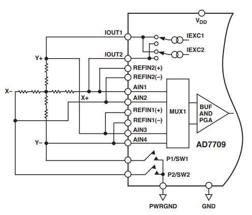
This excitation current is directed to either Y+ or X+ or it can be powered off if the screen has not been touched for some predetermined time. The two low side power switches are used to complete the excitation path by sinking the constant current to ground through either the Y+ or X– Pins.
To make a Y-axis measurement, the two current sources are switched to IOUT1 and the low side power switch P1/SW1 is turned on. The excitation current flows into Y+ and out of Y– to power ground. The Y-axis signal appearing at Pins X+ and X– is measured by the differetial input pair AIN1/AIN2 using the reference input pair of REFIN1(+)/REFIN1(–). Figure H2 shows the active wiring for this Y-axis measurement with the inactive wiring shown in half-tone and the excitation current shown in bold.
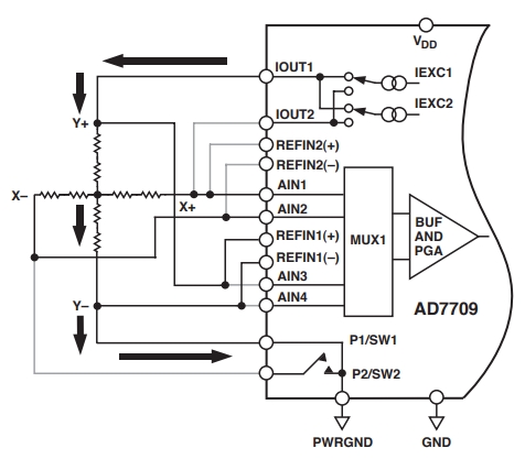
To make an X-axis measurement, the two current sources are switched to IOUT2 and the low side switch P2/SW2 is now turned on. This causes the excitation current to flow into X+ and out of X– to power ground. The X-axis signal appearing at Pins Y+ and Y– is routed to differential input pair AIN3/AIN4 with reference pair REFIN2(+)/REFIN2(–) providing the reference voltage for the conversion. Figure H3 shows active wiring for the X-axis measurement with the excitation current shown in bold and the inactive wiring shown in half-tone.
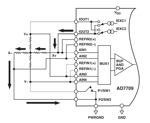
Typical screen impedances range from 900 Ω down to 200 Ω. With an excitation current of 400 µA this will produce full-scale signals from 360 mV down to 80 mV. This will present no problems to the AD7709 since its on-board PGA allows full-scale input signals from VDD down to 20 mV.
I. Driving a Multi-Axis Force Sensor for Position Control
Torque and force sensors based on strain gage technology are used extensively in industrial applications. In the computer industry, cursor control using strain gage-based force sensors has also been well accepted. A good example of this technology is the Aurora series of multi-axis force sensors from Bourns Inc*. A 6 mm perpendicular post connects to a 25 mm × 26 mm ceramic substrate that has screen-printed strain gages placed at strategic locations around the post. When pressure is brought to bear on the top of the post (by a finger), the direction and intensity of that pressure can be detected by changes in the strain gages. The output signals from these force sensors are usually fed to a string of voltage comparators to supply simple up/down and left/right instructions to the system electronics. However, with some more sophisticated signal conditioning, linear X- and Y-axis measurements indicating actual applied force can be easily made. Force measurement in the Z-axis is possible but repeatability is reduced due to sensor attributes.
The sensitivity of the Aurora series sensors in the X and Y dimensions is approximately 1 mV/V; in the Z dimension it is approximately 0.15 mV/V. To ensure as large a signal level as possible, the sensor is excited directly by the power supply voltage. In Figure I1, the X and Y axis of the sensor are modelled as being orthogonal, series-connected pairs of resistors. With no force applied to the post, the resistor pair sensitive to X-axis force, RX1 and RX2, are nominally matched to within ±1% and the output voltage level is nominally VDD/2. Similarly for the Y-axis, with no force applied, the resistor pair, RY1 and RY2, are matched to within ±1% and the output voltage level is again nominally VDD/2. When the post is under strain as a result of finger force, the full-scale output signals from either axis are of the order of ±5 mV sitting on the nominal VDD/2 level. In order to convert these small single-ended signals with as much resolution as possible, it is necessary to turn the single-ended signals into pseudo-differential signals. This is done by programming the analog inputs of the AD7709 to operate as pseudo-differential inputs with respect to a common input pin, termed AINCOM. If AINCOM is also sitting at VDD/2, then the small ±5 mV signals can be plucked from the large dc levels they sit upon. The X-, Y-, and Z-axis signals are fed into analog inputs AIN1, AIN2, and AIN3, respectively.
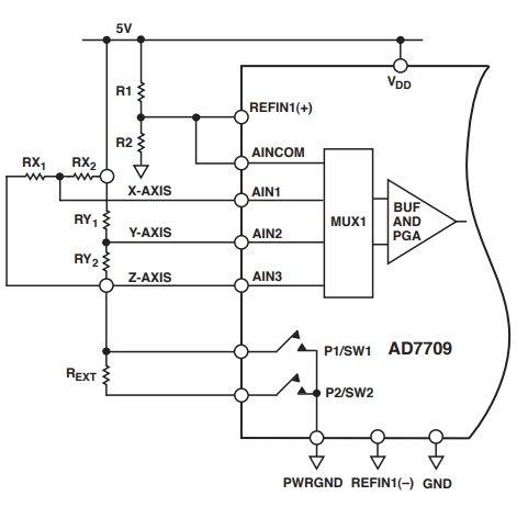
Equal value resistors R1 and R2 bias-up AINCOM to VDD/2. This voltage is also used as the ratiometric reference voltage for the AD7709. If desired, an absolute voltage reference could also be used. All initial errors due to resistor mismatches can be calibrated out by the AD7709 in a calibration cycle.
To measure force or strain in either the X- or Y-axis, the low side switch P1/SW1 is closed placing almost the full power supply across the sensor. Channels AIN1 and AIN2 measure the X- and Y-axis strain, respectively.
To measure strain in the Z-axis, the P1/SW1 switch is opened and the P2/SW2 switch is closed. The Z-axis signal appears on AIN3. The external resistor REXT should have nominally the same value as each of the four sensor resistors or 820 Ω.
If only X- and Y-axis results are important, then this external 820 Ω resistor should be removed and the bottom of R2 removed from ground and placed on the P1/SW1 pin. In addition, the REFIN(–) input should also be removed from ground and repositioned on the P1/SW1 pin. This rearrangement makes the circuit more ratiometric by avoiding any ohmic drops across the low side switch.
J. Use New Synchronous VFCs for Low Side Current Sensing
Voltage-to-frequency converters lend themselves easily to converting current flow into a digital signal that the timer/counter input of a microcomputer (µC) or microprocessor can understand. If electrical isolation is needed between the current flow and the µC, then it is a straightforward task to add a single opto-isolator in the signal chain.
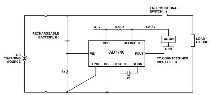
The two circuits presented here demonstrate the use of an AD7740 synchronous VFC for low side current measurements. Figure J1 shows a circuit where the current flow—both into and out of a rechargeable battery—is being monitored. Since the current through the sense resistor, RS, can be bidirectional, a bipolar voltage signal with respect to GND will be developed across RS. The analog input stage of the AD7740 has an input buffer that is turned off in this situation to allow a genuine negative input voltage of up to –150 mV to be processed. Even with the buffer off, however, the input impedance is still of the order of 600 kΩ so the loading effect of this on the sense resistor is negligible. The transfer function for the AD7740 is represented by:
FOUT = 0.1 fCLKIN + 0.8(VIN/VREF) fCLKIN
where fCLKIN is the input clock frequency, VIN is the input voltage, and VREF is the reference voltage used.
In the figure, a low cost 1MHz ceramic resonator—such as a Murata CSBF1000J—is used with the internal oscillator circuit to provide the clock source. Although the VFC has an internal voltage reference of 2.5 V, it is not used in this application since an absolute reading of the current flowing is required. Instead the REFIN/OUT Pin is tied to an AD589 whose output is 1.23 V. Note that if the 3.3 V supplying the AD7740 is tightly regulated, then the REFIN/REFOUT Pin can be tied to VDD directly. With a sense resistor of 100 mΩ, the VFC input voltage varies over ±100 mV with a current flow of ±1 A. Using these conditions, the output frequency varies from 41 kHz with –100 mV input to 170.4 kHz with +100 mV input. At 0 V input, the output frequency is approximately 106 kHz. Thus the output frequency varies by approximately ±64.5 kHz around 106 kHz for an input change of ±100 mV around 0 V or more accurately for a current flow of ±1 A. The accuracy of this circuit is better for positive input voltages, being less than 0.3% of full scale with +100 mV input. For negative input voltages, the accuracy deteriorates for increasingly negative inputs, going out to 2% at –100 mV. The value of the sense resistor is scaled according to the maximum bidirectional currents to be measured. A lower value of sense resistor will allow higher currents to be monitored.
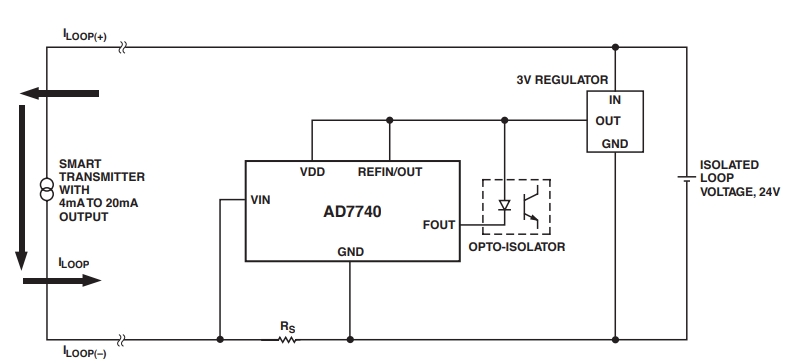
The second circuit shows a VFC being used in an isolated 4 mA to 20 mA receiver circuit. In Figure J2, an isolated loop voltage of 24 V drives a remote 4 mA to 20 mA smart transmitter. Typical transmitters measure pressure or temperature in an industrial process and are generally loop-powered. They transmit their measurement result back to the control room by modulating the current flow in the loop: 4 mA indicating zero scale and 20 mA indicating full scale, for instance.
In Figure J2 the loop current, ILOOP, flows through the sense resistor, RS, generating a voltage input signal for the VFC. The value of RS will determine the input full-scale signal. In a very noisy environment, it might be best to strive for as large a full-scale signal as possible. A usual value for RS would be 125 Ω. With the REFIN/REFOUT Pin tied to VDD, the maximum input voltage the AD7740 can accept is VDD with the device's input buffer turned off.
The output pulse stream pulses the LED of an opto-isolator to transfer the measurement from the isolated floating measurement side to the nonisolated control room side.
著者について
この記事に関して
製品
製造中
24ビットA/Dコンバータ、電流源付き、CMOS、シグナル・コンディショニング
製造中
24ビットA/Dコンバータ、ΣΔ型、2チャンネル・アナログ入力付き、CMOS、シグナル・コンディショニング
製造中
24ビットA/Dコンバータ、ΣΔ型、CMOS、3V/5V、500µA
リファレンス電圧、超高精度低ノイズ2.500V XFET®
電圧リファレンス、1.2V、2端子
タッチ・スクリーン・デジタイザ
タッチスクリーン・デジタイザ
レギュレータ、低ドロップアウト、高精度、超低静止電流、300mA、anyCAP®
VF(電圧 / 周波数)コンバータ、3V / 5V低電圧電源動作、同期型
24ビットA/Dコンバータ、ΣΔ型、ブリッジ・トランスデューサ・アプリケーション向、CMOS、低消費電力
24ビットA/Dコンバータ、ΣΔ型、高速チャンネル間セトリング・タイム、CMOS、低ノイズ
16ビットA/Dコンバータ、ΣΔ型、電流源 / スイッチ可能電圧リファレンス入力 / 入出力ポート付き
16/24ビットA/Dコンバータ、ΣΔ型、低電圧、低消費電力、デュアル
A/Dコンバータ、12ビット/16ビット、312.5KHz/468.5KHz、シグマ・デルタ型、CMOS
16ビットA/Dコンバータ、ΣΔ型、CMOS、1.2MSPS
16ビットA/Dコンバータ、ΣΔ型、8/10チャンネル、低電圧、低消費電力
24ビットA/Dコンバータ、ΣΔ型、マッチングされたRTD電流源付き、CMOS、低消費電力、シグナル・コンディショニング
一致したRTD励起電流出力を持つシグマ・デルタ・シグナル・コンディショニング24ビットCMOS ADC
A/Dコンバータ、24ビット、4チャンネル、±10V入力範囲、高速スループット、シグマ・デルタ型
A/Dコンバータ、24ビット、8チャンネル、8.5 KHz、シグマ・デルタ型
A/Dコンバータ、24ビット分解能、 2チャンネル、±10V入力範囲、高速スループット、シグマ・デルタ
16ビットA/Dコンバータ、ΣΔ型、3V/5V、450µA
A/Dコンバータ、24ビット分解能、 2チャンネル、±10V入力範囲、高速スループット、シグマ・デルタ
16ビットA/Dコンバータ、ΣΔ型、3V/5V、450µA
24ビットA/Dコンバータ、ΣΔ型、ロードセル・アプリケーション向け、CMOS、ブリッジ・トランスデューサ
16ビットA/Dコンバータ、ΣΔ型、3V/5V、1mW、3チャンネル擬似差動
16ビットA/Dコンバータ、パラレル読出し構造、モノリシック
16ビットA/Dコンバータ、ΣΔ型、3V / 5V、1mW、2チャンネル差動
ΣΔ型変調器、90dBダイナミック・レンジ、CMOS
CMOS、16ビット、195 kSPS、シグマ・デルタ型ADC
24 ビット、8/10 チャンネル、低電圧、低消費電力シグマ・デルタ ADC
ΣΔ型変調器、7次、デュアル
24ビットA/Dコンバータ、ΣΔ型、RTD電流源付き、CMOS、シグナル・コンディショニング
16ビットA/Dコンバータ、バイト読出し構造、モノリシック
A/Dコンバータ、16ビット、3チャンネル、シグマ・デルタ型、3V/5V/±10V入力範囲、1mW