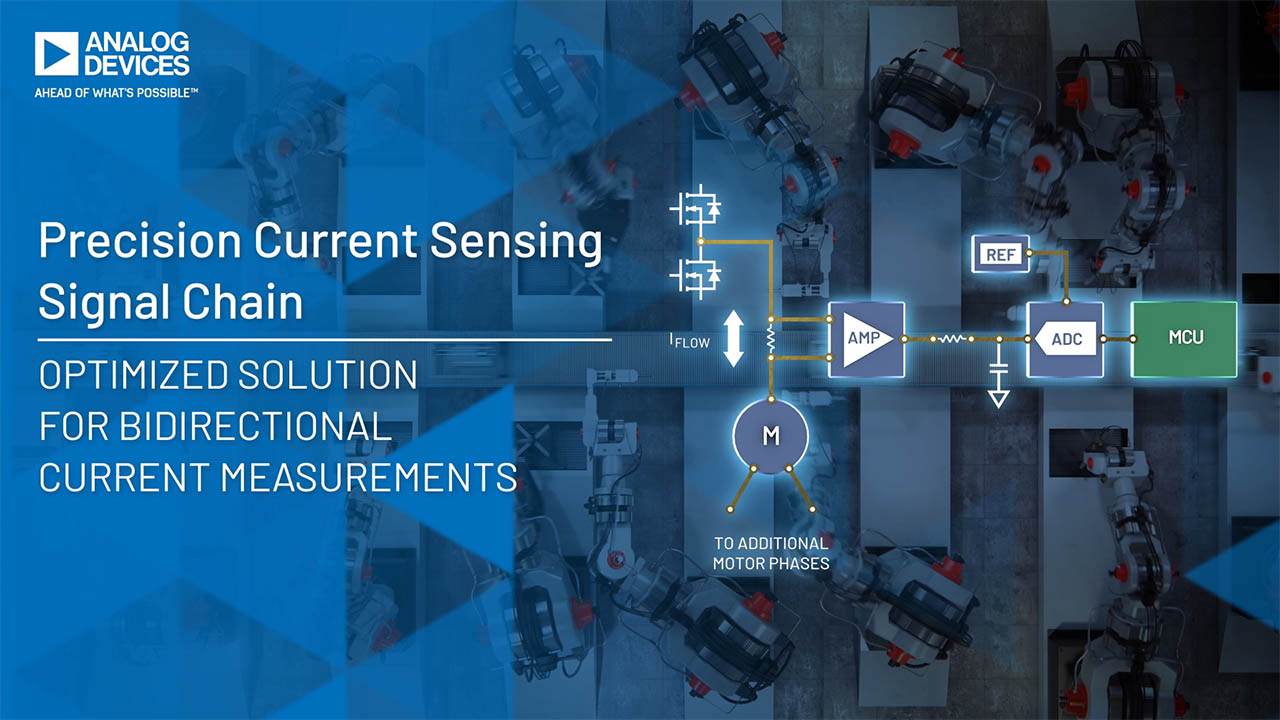
Save time and deliver your solutions faster with ADI’s new suite of precision technology signal chains. Align your applications ranging from Smart Industry to Instrumentation, Electrification to Digital Health, to exactly the right precision technology combinations.
Tailor your signal chain with confidenceADR4550
PRODUCTIONUltra-Low-Noise, High-Accuracy 5.0V Voltage Reference
- Part Models
- 8
- 1ku List Price
- Starting From $3.32
Overview
- Maximum temperature coefficient (TCVOUT):
- 0.8 ppm/°C (D grade 0°C to 70°C)
- 1 ppm/°C (C grade 0°C to 70°C)
- 2 ppm/°C (B grade −40°C to +125°C)
- 4 ppm/°C (A grade −40°C to +125°C)
- Output noise (0.1 Hz to 10 Hz):
- 1 μV p-p at VOUT of 2.048 V typical
- Initial output voltage error:
- B, C, D grade: ±0.02% (maximum)
- Input voltage range: 3 V to 15 V
- Operating temperature:
- A grade and B grade: −40°C to +125°C
- C grade: 0°C to +70°C
- Output current: +10 mA source/−10 mA sink
- Low quiescent current: 950 μA (maximum)
- Low dropout voltage: 300 mV at 2 mA (VOUT ≥ 3 V)
- 8-lead SOIC package and LCC package
- AEC-Q100 qualified for automotive applications
- Long-term drift: 8 ppm typical at 4500 hours
The ADR4520/ADR4525/ADR4530/ADR4533/ADR4540/ADR4550 devices are high precision, low power, low noise voltage references featuring ±0.02% B, C, and D grade maximum initial error, excellent temperature stability, and low output noise.
This family of voltage references uses an innovative core topology to achieve high accuracy while offering industry-leading temperature stability and noise performance. The low, thermally induced output voltage hysteresis and low long-term output voltage drift of the devices also improve system accuracy over time and temperature variations.
A maximum operating current of 950 μA and a maximum low dropout voltage of 300 mV allow the devices to function very well in portable equipment.
The ADR4520/ADR4525/ADR4530/ADR4533/ADR4540/ADR4550 series of references are each provided in an 8-lead SOIC and are available in a wide range of output voltages, all of which are specified over the extended industrial temperature range of −40°C to +125°C.
The ADR4525, ADR4540, and ADR4550 are also available in D, which are in 8 lead LCC package, and C grade with a temperature range of 0°C to 70°C. The ADR4525W, available in an 8‑lead SOIC package, is qualified for automotive applications.
Applications
- Precision data acquisition systems
- High resolution data converters
- High precision measurement devices
- Industrial instrumentation
- Medical devices
- Automotive battery monitoring
Documentation
Data Sheet 1
Technical Articles 5
Video 1
Circuit Note 5
3rd Party Solutions 1
Analog Dialogue 2
Rarely Asked Question 1
ADI has always placed the highest emphasis on delivering products that meet the maximum levels of quality and reliability. We achieve this by incorporating quality and reliability checks in every scope of product and process design, and in the manufacturing process as well. "Zero defects" for shipped products is always our goal. View our quality and reliability program and certifications for more information.
| Part Model | Pin/Package Drawing | Documentation | CAD Symbols, Footprints, and 3D Models |
|---|---|---|---|
| ADR4550ARZ | 8-Lead SOIC | ||
| ADR4550ARZ-R7 | 8-Lead SOIC | ||
| ADR4550BRZ | 8-Lead SOIC | ||
| ADR4550BRZ-R7 | 8-Lead SOIC | ||
| ADR4550CRZ | 8-Lead SOIC | ||
| ADR4550CRZ-R7 | 8-Lead SOIC | ||
| ADR4550DEZ | 8-Terminal LCC (5 mm x 5 mm x 1.45 mm) | ||
| ADR4550DEZ-R7 | 8-Terminal LCC (5 mm x 5 mm x 1.45 mm) |
This is the most up-to-date revision of the Data Sheet.
Hardware Ecosystem
| Parts | Product Life Cycle | Description |
|---|---|---|
| LDO Linear Regulators 1 | ||
| LT3040 | RECOMMENDED FOR NEW DESIGNS | 20V, 200mA, Ultralow Noise, Ultrahigh PSRR Precision DAC/Reference Buffer |
Tools & Simulations
LTspice
Models for the following parts are available in LTspice:
- ADR4550
ADI Circuit Explorer™
ADI Circuit Explorer™ uses AI to interpret natural language prompts and search a database of validated analog circuit designs, helping you quickly find the best match for your needs.
Open ToolSignal Chain Designer
Signal Chain Designer is a web-based tool designed to create and simulate complex precision signal chains. See your circuit’s performance before you commit to your PCB: transfer function, noise, power consumption, input range, and DC error. Quickly experiment with different parts and architectures. Signal chains can be exported to LTspice for further analysis.
Open ToolLTspice® is a powerful, fast and free simulation software, schematic capture and waveform viewer with enhancements and models for improving the simulation of analog circuits.


