AD4085
推荐用于新设计16-Bit, 10 MSPS, Low Noise, Low Power SAR ADC
Low Noise, Low Power, Fast Precision SAR ADC
- 产品模型
- 3
概述
- 16-bit resolution, no missing codes
- Throughput: 10MSPS, 131.25ns conversion latency
- Noise spectral density: 20.85nV/√Hz,−160.1dBFS/Hz
- Low 1/f, low frequency noise (0.1Hz to 10Hz): 206.4nV rms
- Low power: 57.8mW typical at 10MSPS
- INL: ±5ppm (typ), ±10ppm (max)
- Dynamic range: 93.2dBFS
- SNR/THD
- 92.9dB (typ)/−114dB (typ) at fIN = 1kHz
- 92.5dB (typ)/−102.9dB (typ) at fIN = 1MHz
- Easy Drive
- 6V p-p differential input range
- Continuous signal acquisition
- Linearized, 5μA/MSPS input current
- Integrated, low-drift reference buffer and decoupling
- Integrated VCM generation
- Digital features and data interface
- Conversion result FIFO, 16K sample depth
- Digital averaging filter with up to 210 decimation
- SPI configuration
- Configurable data interface
- Single lane, DDR, serial LVDS, 160Mbps per lane
- Dual lane, DDR, serial LVDS, 80Mbps per lane
- Single/quad lane SPI data interface
- Package
- 49-ball, 5mm × 5mm CSP_BGA, 0.65mm pitch
- Integrated supply decoupling capacitors
- Operating temperature range: −40°C to +85°C
The AD4085 is a high speed, low noise, low distortion, 16-bit, Easy Drive, successive approximation register (SAR) analog-to-digital converter (ADC). Maintaining high performance (signal-to-noise and distortion (SINAD) ratio > 92dBFS) at signal frequencies in excess of 1MHz enables the AD4085 to service a wide variety of precision, wide bandwidth data acquisition applications. Simplification of the input anti-alias filter design can be accomplished by applying oversampling along with the integrated digital filtering and decimation to reduce noise and lower the output data rate for applications that do not require the lowest latency of the AD4085.
The AD4085 Easy Drive features reduce both signal chain complexity and power consumption while enabling greater channel density and flexibility in companion component selection. The product input structure was designed to minimize any input dependent signal currents, therefore reducing any converter induced settling artifacts. The continuous acquisition architecture allows settling across the entire conversion cycle, easing ADC driver settling and bandwidth requirements as compared to other high-speed data converters.
The AD4085 includes several elements that simplify data converter integration: a low drift reference buffer, low dropout (LDO) regulators to generate ADC core and digital interface supply rails, and a 16K result data first-in first out (FIFO) that can greatly reduce the load on the digital host. Additionally, critical supply and reference decoupling capacitors are integrated in the package to ensure optimum performance, simplify printed circuit board (PCB) layout, and reduce the overall solution footprint.
APPLICATIONS
- Digital imaging
- Cell analysis
- Spectroscopy
- Automated test equipment
- High speed data acquisition
- Digital control loops, hardware in the loop
- Power quality analysis
- Source measurement units
- Electron and X-ray microscopy
- Radar level measurement
- Nondestructive test
参考资料
数据手册 1
用户手册 1
视频 1

器件驱动器 1
在线研讨会 2
ADI 始终高度重视提供符合最高质量和可靠性水平的产品。我们通过将质量和可靠性检查纳入产品和工艺设计的各个范围以及制造过程来实现这一目标。出货产品的“零缺陷”始终是我们的目标。查看我们的质量和可靠性计划和认证以了解更多信息。
| 产品型号 | 引脚/封装图-中文版 | 文档 | CAD 符号,脚注和 3D模型 |
|---|---|---|---|
| AD4085BBCZ | 49-ball CSP_BGA (5 mm x 5 mm x 1.33 mm) | ||
| AD4085BBCZ-RL | 49-ball CSP_BGA (5 mm x 5 mm x 1.33 mm) | ||
| AD4085BBCZ-RL7 | 49-ball CSP_BGA (5 mm x 5 mm x 1.33 mm) |
这是最新版本的数据手册
软件资源
Evaluation Software 4
找不到您所需的软件或驱动?
硬件生态系统
| 部分模型 | 产品周期 | 描述 |
|---|---|---|
| 差分放大器 2 | ||
| ADA4945-1 | 推荐用于新设计 | 高速、±0.3µV/°C 失调漂移、全差分 ADC 驱动器 |
| ADA4930-1 | 推荐用于新设计 | 超低噪声驱动器,适用于低压ADC |
| 电源系统管理(PSM)和时序控制器 1 | ||
| ADM1085 | 量产 | 内置高电平有效、开漏使能输出的电压时序控制器 |
| 基准电压源 2 | ||
| LTC6655 | 量产 | 0.25ppm 噪声、低漂移、精准基准系列 |
| ADR4530 | 量产 | 超低噪声、高精度3.0V基准电压源 |
| 监控电路和复位器IC 1 | ||
| MAX16061 | 推荐用于新设计 | 1%精度、四/六/八路电压µP监控电路 |
| 开关稳压器和控制器 3 | ||
|
LT8604/ LT8604C |
高效42V/120mA同步降压 | |
| LT8606 | 推荐用于新设计 | 具有 2.5μA 静态电流的 42V、350mA 同步降压型稳压器 |
| MAX1606 | 量产 | 具有True Shutdown™功能的28V内部开关LCD偏置电源 |
| 扇出缓冲器和分路器 1 | ||
| AD9508 | 推荐用于新设计 | 1.65 GHz时钟扇出缓冲器,集成输出分频器和延迟调整 |
| 锁相环(PLL)频率合成器 1 | ||
| ADF4350 | 量产 | 集成VCO的宽带频率合成器 |
| 线性稳压器 6 | ||
| MAX38912 | 推荐用于新设计 | 具有低功耗模式的11µVRMS低噪声、500mA LDO线性稳压器 |
| LT3045 | 推荐用于新设计 | 20V、500mA、超低噪声、超高 PSRR 线性稳压器 |
| ADP150 | 量产 | 超低噪声、150 mA CMOS线性调节器 |
| ADP7182 | 推荐用于新设计 | -28 V、 −200 mA、,低噪声、线性稳压器 |
| ADP7118 | 推荐用于新设计 | 20 V、200 mA、低噪声、CMOS LDO线性稳压器 |
| LT3093 | 推荐用于新设计 | –20V、200mA、超低噪声、超高 PSRR 负线性稳压器 |
| 运算放大器 1 | ||
| ADA4899-1 | 量产 | 单位增益稳定、超低失真、1 nV/√Hz电压噪声、高速运算放大器 |
工具及仿真模型
IBIS 模型 1
评估套件


评估 AD4083/AD4084 16 位、40/20 MSPS、差分 SAR ADC
资料


评估 AD4080 快速精密 20 位、40MSPS 差分 SAR ADC
资料
软件


Mixed-Mode Signal Chain Active Learning Module
资料
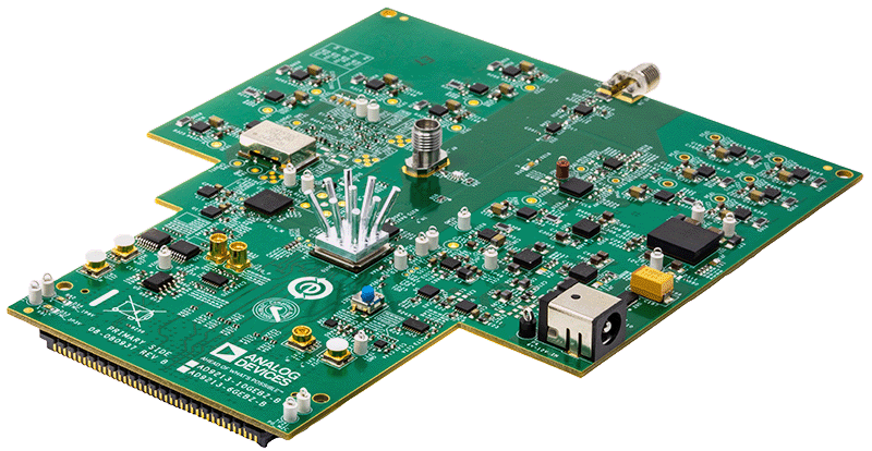
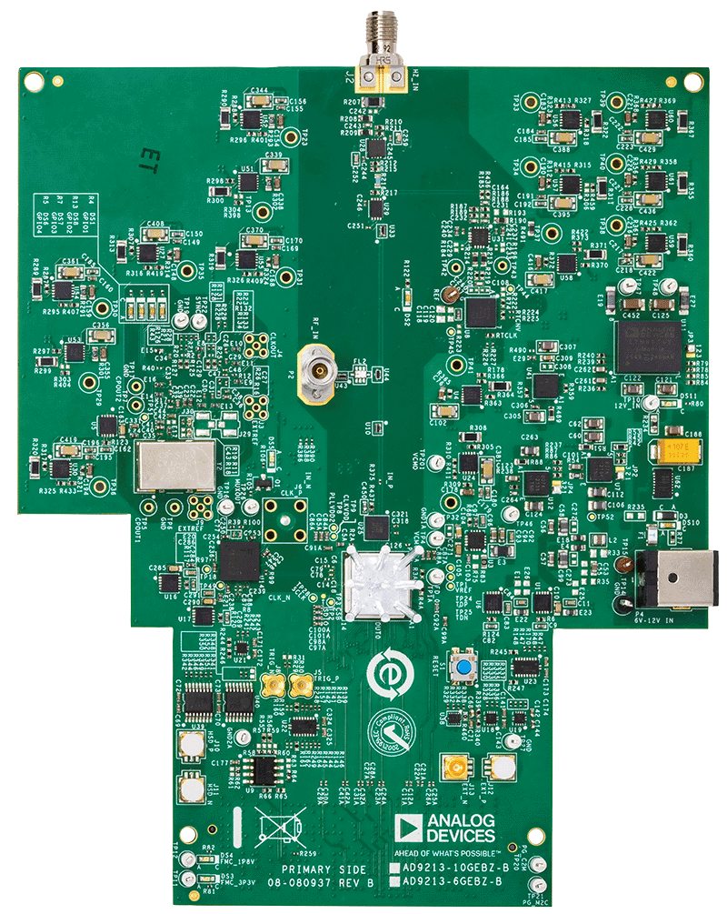
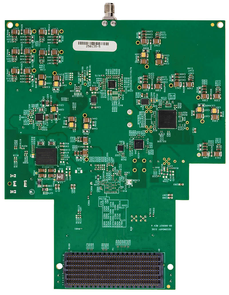
直流耦合10GSPS数字化仪评估板
资料
软件
最新评论
需要发起讨论吗? 没有关于 AD4085的相关讨论?是否需要发起讨论?
在EngineerZone®上发起讨论