ADRV9042
推荐用于新设计8T8R SoC with DFE, 400 MHz iBW RF Transceiver
- 产品模型
- 2
概述
- Highly integrated transceiver
- 8 transmit (Tx), 8 receive (Rx), and 2 observation receivers (ORx)
- LO tuning range: 600 MHz to 7125 MHz
- RF range: 500 MHz to 7455 MHz1
- Zero-IF architecture reduces system size, weight, and power (SWaP)
- Initial and run time calibrations maintain high performance
- Dual fully integrated fractional-N RF synthesizers
- Dual external LO inputs supporting operation up to 6 GHz.
- Multichip phase synchronization for all local oscillator (LO) and baseband clocks
- Single and multiband (N × 2T2R/4T4R) capability
- 4 individual band profiles within tunable range (band profiles define bandwidth and aggregate sampling rate of a channel)
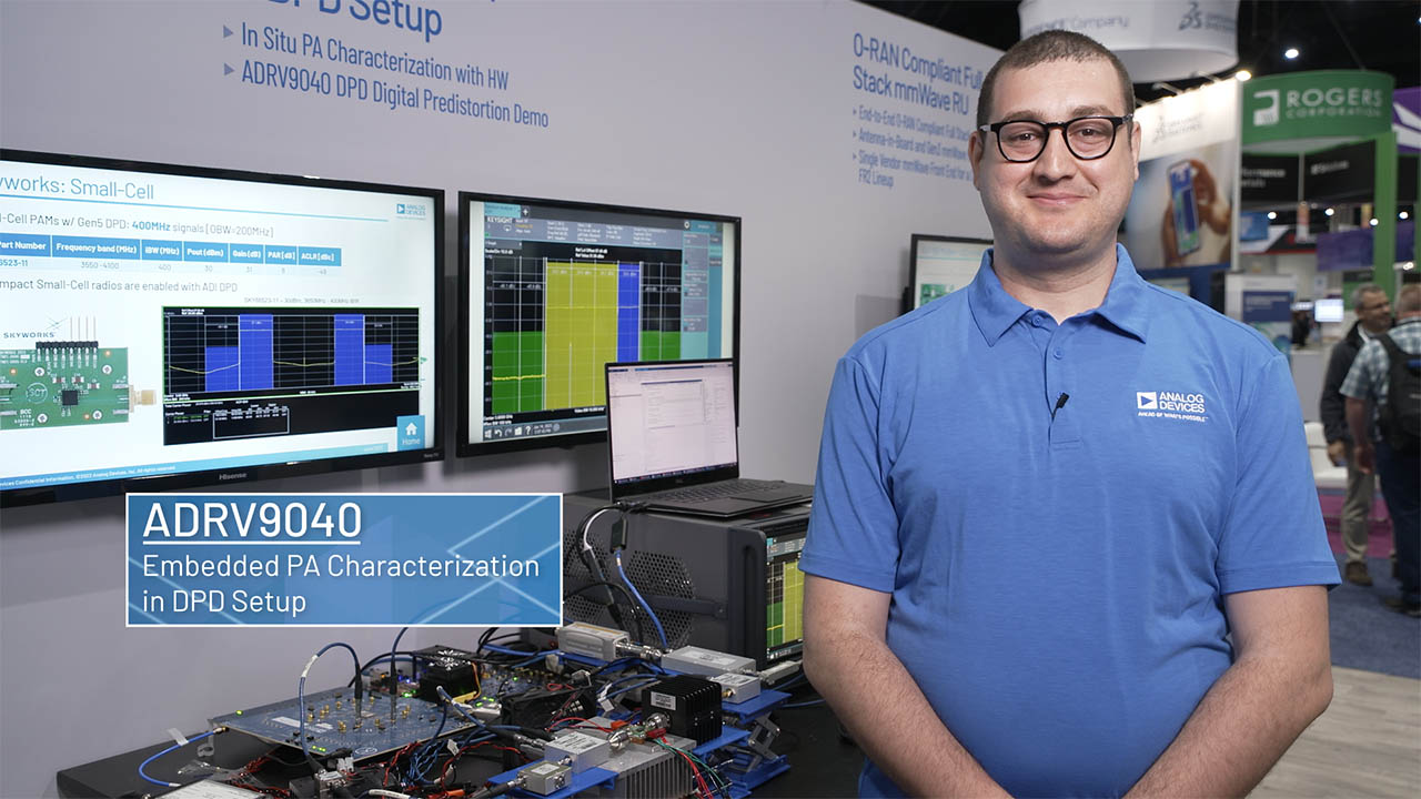
- Fully integrated DPD supporting up to 400 MHz iBW/OBW
- Supports up to 660 MHz instantaneous BW, 400 MHz occupied BW on RF front end with DFE enabled
- Supports up to 400 MHz instantaneous/occupied BW with DFE disabled
- Supports JESD204B and JESD204C digital interface
- Simplifying thermal and power consumption challenges
- 10.44 W power consumption for the TDD mode, full DFE features enabled use case with 100 MHz iBW/OBW2
- 125°C maximum junction temperature for intermittent operation, 110°C for continuous (operating lifetime impact at >110°C can be offset by operation at <110°C based on acceleration factors)
- Fully integrated DFE (DPD, CDUC, CDDC, and CFR) engine reduces FPGA resources, halves SERDES lane rate, and simplifies designs
- DPD adaptation engine for power amplifier linearization
- CDUC/CDDC—maximum of 8 component carriers (CCs) per each transmitter/receiver channel
- Multistage CFR engine
- Low power monitor and sleep modes
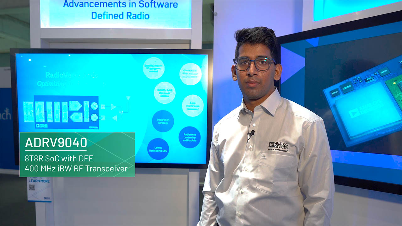
The ADRV9042 is a highly integrated, RF transceiver with an integrated, digital front end (DFE) designed for use in instrumentation and aerospace, defense applications, and advanced communications systems. The transceiver contains eight transmitters, two observation receivers, eight receivers, integrated LO and clock synthesizers, and digital signal processing functions. The ADRV9042 is a high performance and low power radio with DFE support that has been designed for use in general-purpose applications operating from low frequencies. The ADRV9042 has a tuning range from 600 MHz to 7125 MHz and covers all UHF, industrial, scientific, and medical (ISM) and cellular frequency bands including WiFi 6E. Support beyond these frequencies can be enabled via external upconverters and downconverters available at Analog Devices, Inc.
Please see the Data Sheet for the full description.
APPLICATIONS
- Tactical communications
- Phased array radars
- Electronic warfare
- Wireless test and measurement
- Portable instruments
- Time division duplexing (TDD)
- Frequency division duplexing (FDD)
参考资料
数据手册 1
用户手册 1
应用笔记 7
技术文章 3
产品亮点 1
视频 2
产品亮点 1
非常见问题 1
模拟对话 2
ADI 始终高度重视提供符合最高质量和可靠性水平的产品。我们通过将质量和可靠性检查纳入产品和工艺设计的各个范围以及制造过程来实现这一目标。出货产品的“零缺陷”始终是我们的目标。查看我们的质量和可靠性计划和认证以了解更多信息。
| 产品型号 | 引脚/封装图-中文版 | 文档 | CAD 符号,脚注和 3D模型 |
|---|---|---|---|
| ADRV9042BBPZ-8T1 | 736-Ball BGA_ED (27mm x 20 mm x 1.994 mm) | ||
| ADRV9042BBPZRL-8T1 | 736-Ball BGA_ED (27mm x 20 mm x 1.994 mm) |
这是最新版本的数据手册
软件资源
API Device Drivers 1
Device Application Programming Interface (API) C code drivers provided as reference code allows the user to quickly configure the product using high-level function calls. The library acts as an abstraction layer between the application and the hardware. The API is developed in C99 to ensure agnostic processor and operating system integration. Customers can port this application layer code to their embedded systems/ Baseband Processor by integrating their platform-specific code base to the API HAL layer. To request this software package, go to the Software Request Form signed in with your MyAnalog account and under “Target Technology option - select “Wireless Communications" and choose processor/SOC as "ADRV9040 or ADRV9044" , select the check box as well and submit the form. You will receive an email notification with a link for software download.
Evaluation Software 1
找不到您所需的软件或驱动?
硬件生态系统
| 部分模型 | 产品周期 | 描述 |
|---|---|---|
| RF放大器 2 | ||
| ADRF5515A | 推荐用于新设计 | 双通道,3.3 GHz至4.0 GHz,20 W接收器前端 |
| ADRF5515 | 推荐用于新设计 |
双通道,3.3 GHz至4.0 GHz,20 W接收器前端 |
| RF开关 1 | ||
| ADRF5250 | 推荐用于新设计 | 0.1 GHz至6 GHz硅SP5T开关 |
| 低噪声放大器(LNA)和功率放大器 2 | ||
| ADL5545 | 推荐用于新设计 | 30 MHz 至 6 GHz RF/IF 增益模块 |
| ADL5611 | 推荐用于新设计 | 30 MHz 至6 GHz RF/IF增益模块 |
| 开关稳压器和控制器 5 | ||
| ADP5056 | 推荐用于新设计 | 集成式三通道降压调节器电源解决方案 |
| LT8627SP | 推荐用于新设计 | 具有超低噪声的18V/16A降压型Silent Switcher 3 |
| LT83205 | 推荐用于新设计 | 具有超低噪声基准电压源的 18V、5A 降压型 Silent Switcher 3 |
| MAX20840T | 量产 | 具有 PMBus 的 40A、2MHz、2.7V 至 16V 集成降压开关稳压器 |
|
LT8625SP/ LT8625SP-1 |
具有超低噪声基准电压源的18V/8A降压型Silent Switcher 3 | |
| 时钟IC 2 | ||
| AD9528 | 推荐用于新设计 | 提供14路LVDS/HSTL输出的JESD204B/JESD204C时钟发生器 |
| AD9545 | 推荐用于新设计 | IEEE1588 第 2 版以及 1 pps 同步器和自适应时钟转换器 |
工具及仿真模型
SDR Integrated Transceiver Design Resources
This site contains the device documentation packages for the SDR Integrated Transceivers including user guides, IBIS models, and PCB files.
打开工具ADIsimRF
ADIsimRF是一款简单易用的RF信号链计算工具。可以计算和导出多达50级的信号链级联增益、噪声、失真和功耗并绘制其曲线。ADIsimRF还包括丰富的ADI射频和混合信号元件的器件模型数据库。
打开工具评估套件


资料
软件


ADS10-V1EBZ Evaluation Board
资料
最新评论
需要发起讨论吗? 没有关于 ADRV9042的相关讨论?是否需要发起讨论?
在EngineerZone®上发起讨论