AN-2600: Multiband Applications—RF Transceivers
Scope
This application note covers the details in using the ADRV9040 for multiband applications. More details on the ADRV9040 are available in datasheet, system development user guide (SDUG), and various application notes in Appendix section.
Introduction
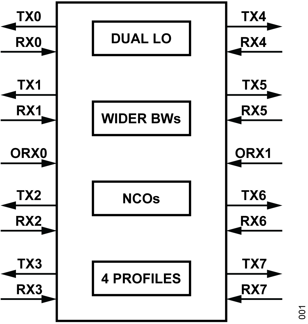
In the ADRV9040 8T8R2O RF transceiver, multiband capability is enabled by dual LO functionality and their additional LO dividers within the path, which allows wideband operation of the receiver and transmitter channels. This allows 4 individual band profiles within the tunable range, it maximizes use case flexibility. Figure 1 shows the overview of its features which enable multiband operation.

Multiband Introduction
The ADRV9040 transceiver supports 8T8R2ORX channels which are independent to each other. However, in some cases, users may not need all 8 transmitter/receiver channels working for the same band depending on the data rate, deployment scenarios and they may have license for other bands as well which means customers can have multibands in the same RRH/ RU without the need of going for an additional RU that must support other bands.
Instead of using 8T8R single band, user can configure 2x 4T4R in a single RRH or 4x 2T2R band combinations as required.
ADRV9040 for Multiband Applications.
The ADRV9040 supports multiband due to its important features as defined below:
- Supports dual LO with variable root and leaf dividers, its ability to multiplex the LO to different transmitter, receiver, and ORX channels
- Wider RF bandwidths for transmitter, receiver, and observation receiver channels
- NCOs with in BDUC/BDDC, CDUC/CDDC blocks
- Ability to configure 4 different profiles
As the ADRV9040 supports wider bandwidth (BW) of 400MHz, if two bands are close to each other and if the front end supports a wider BW combining both the bands which falls within the supported 400MHz BW, there are no changes in the radio small signal design,which is an added advantage.
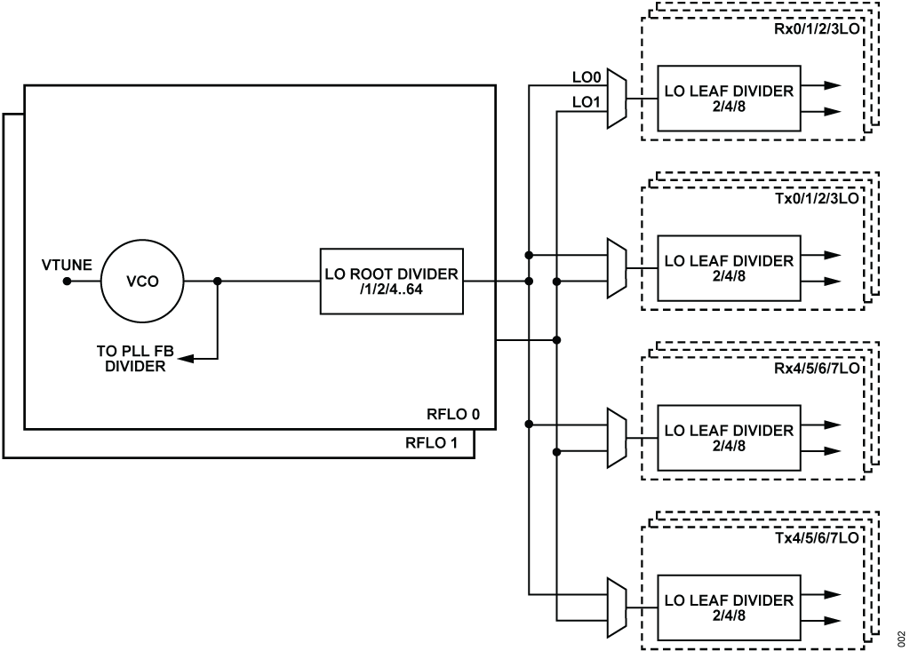
Dual LO with Variable Root and Leaf Dividers
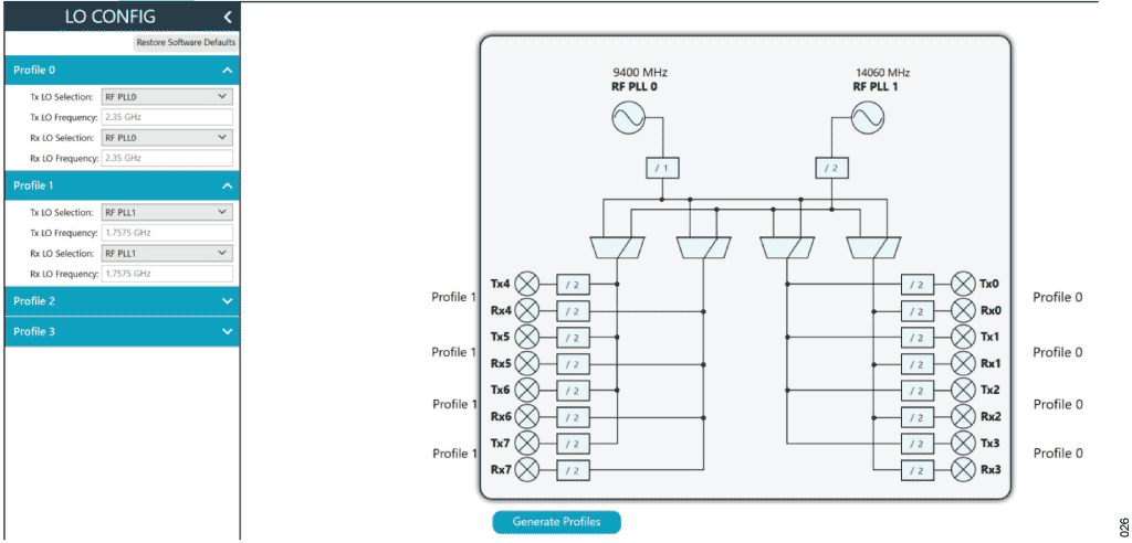
A highly configurable LO generation network is implemented in the device to provide flexibility in LO assignment for the two RF LO sources. The LOGEN network is shown in Figure 2 and consists of a root divider located close to the RF voltage controlled oscillator (RFVCO) and separate leaf dividers located at each receiver and transmitter slice. The root divider ratio is from 1/2/4/8/16/32 64 in binary steps. The leaf divider range is 2/4/8. This setup allows the generation of power of two LO in each transmitter and receiver path and also non-power of 2 LOs in either 4T4R section.
For example, in a multiband setup, where user wants to generate a 3.5GHz LO for a 4T4R section, 1.8GHz for 2T2R and 900MHz for the remaining 2T2R, the RF LOs could be configured as follows:
- To generate the 3.5GHz for transmitter/receiver 0-3, RFLO1 voltage controlled oscillator (VCO) is programmed to 14GHz followed by divide by 4, where root divider = 2 and leaf divider = 2.
- To generate the 1.8GHz for transmitter/receiver 4-5, RFLO2 VCO is programmed to 7.2GHz followed by divide by 4, where root divider = 2 and leaf divider = 2.
- To generate the 900MHz for transmitter/receiver 6-7, RFLO2 VCO is programmed to 7.2GHz followed by divide by 8, where root divider = 2 and leaf divider = 4.
In many cases, given the wide bandwidth of the ADRV9040, a single RF local oscillator (RFLO) in combination with the on-chip NCOs can be sufficient to support several multiband configurations. In this case the unused RFLO can be powered down to save power.
Note that it is not recommended to set RFLO1 = RFLO2, this may cause unwanted coupling between the two PLLs. If a common RFLO is desired, either of RFPLL1 or RFPLL2 must be set to the desired frequency and muxed to both TxLO and RxLO. The configuration must be set to either TXLO = RXLO = RFLO1 or TXLO = RXLO = RFLO2 with the unused RFLO powered down.

Wider RF Bandwidths for Transmitter, Receiver and Observation Receiver Channels
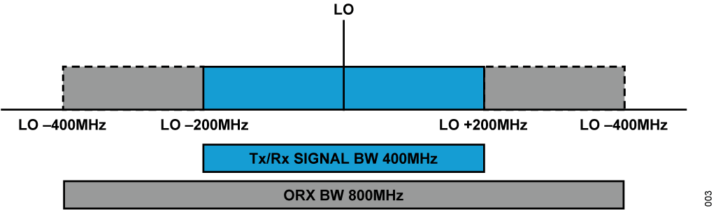
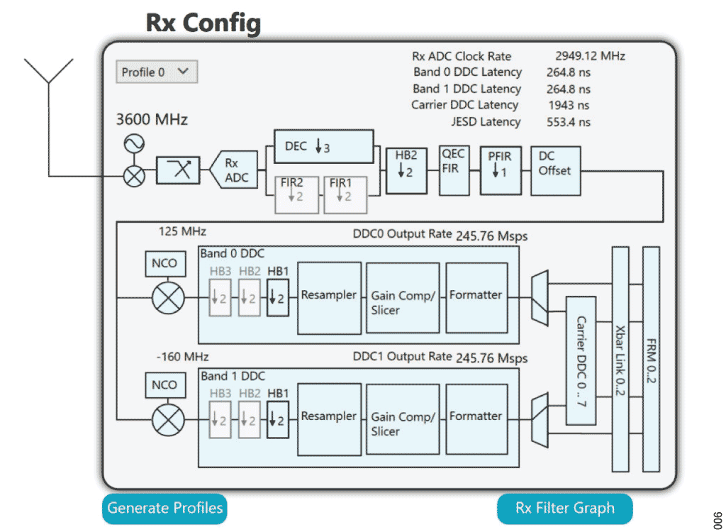
The advantage of ADRV9040 transceiver is its wider bandwidth support. Each transmitter/receiver channel supports 400MHz of Bandwidth. With CDUC/CDDC bypassed, the maximum iBW/OBW supported is 400MHz and with carrier digital upconverter (CDUC)/ carrier digital downconverter (CDDC)enabled, the maximum BW possible is 660MHz and occupied bandwidth (OBW) supported is 400MHz. Figure 3 shows the BW representation of ADRV9040 with respect to the LO frequency.
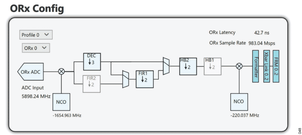
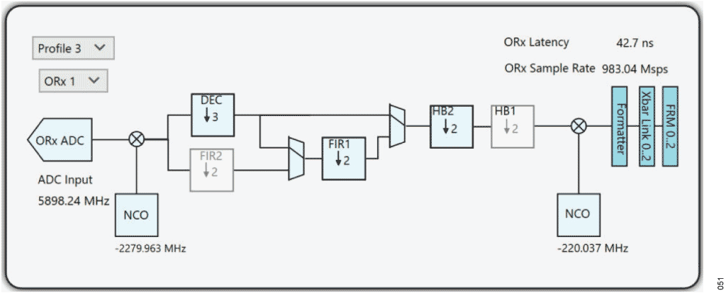
The observation receiver channel has 800MHz of wide BW, which is used for monitoring purpose and for local oscillator leakage (LOL), digital pre-distortion (DPD) tracking calibrations.

NCOS with in BDUC/BDDC, CDUC/CDDC Blocks
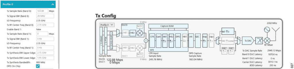
In the band digital up conversion (BDUC)/band digital down conversion (BDDC) blocks, there is an NCO which is used to place the carriers at the appropriate place. Depending on the input rate to the NCO, the maximum frequency range of the numerically controlled oscillator (NCO) can go up to 1GHz.
Similarly, there is an NCO in carrier digital up conversion (CDUC)/ carrier digital down conversion (CDDC) block, which is as well used to place the carriers at the appropriate place in combination with setting BDUC/BDDC NCO frequency as necessary.
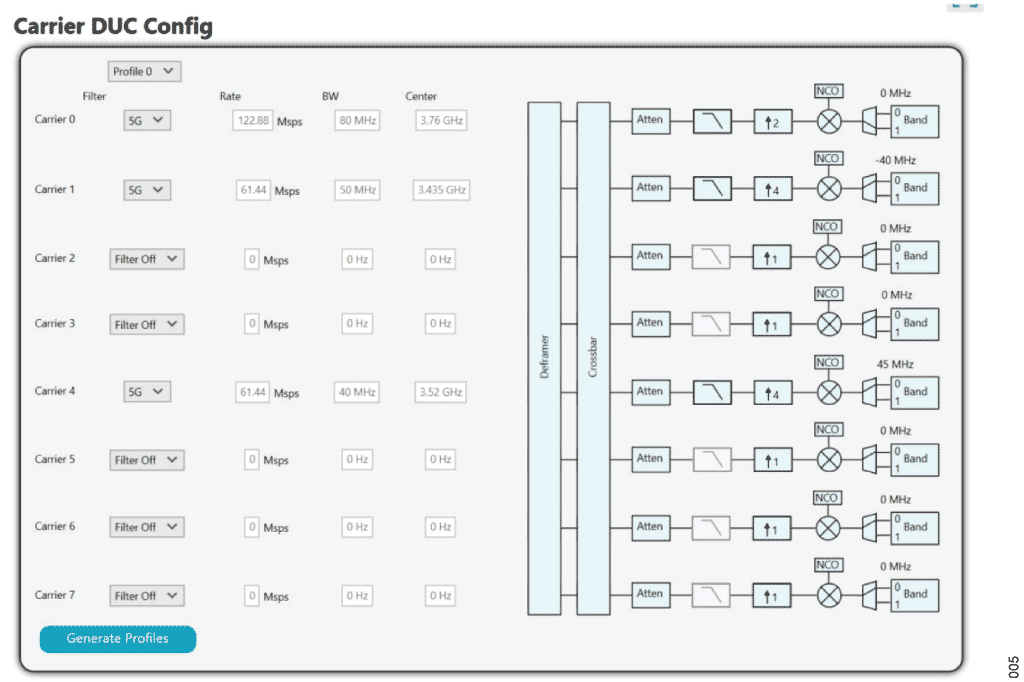
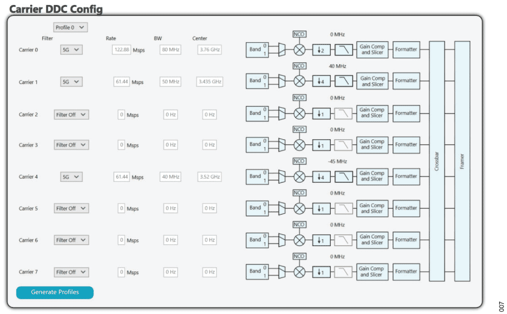
Given below are the figures wherein for UC75, as part of the transmitter path, the BDUC NCO and CDUC NCOs are configured at different frequencies to get to the appropriate carrier frequencies. The same approach is followed for receiver path as well by configuring BDDC and CDC NCOs. Table 1 shows the NCO frequencies that are used to achieve the ultimate carrier frequencies.
| LO Frequency | 3600 | ||
| Carrier | BDUC NCO | CDUC NCO | Carrier Center Frequency |
| C0 | 160 | 0 | 3760 |
| C1 | −125 | −40 | 3435 |
| C4 | −125 | 45 | 3520 |
Figure 4 shows the BDUC NCO placement in the transmitter path and their frequencies used to arrive at the final carrier frequencies.

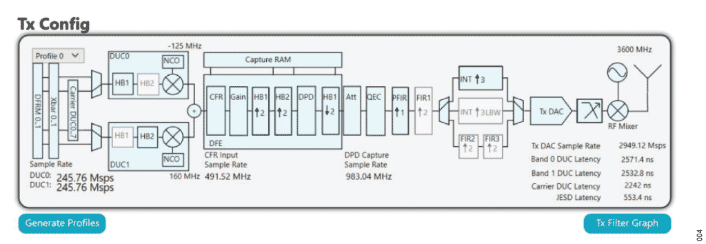
Figure 5 shows the CDUC NCO placement in the CDUC block of the transmitter path and their frequencies used to arrive at the final carrier frequencies.


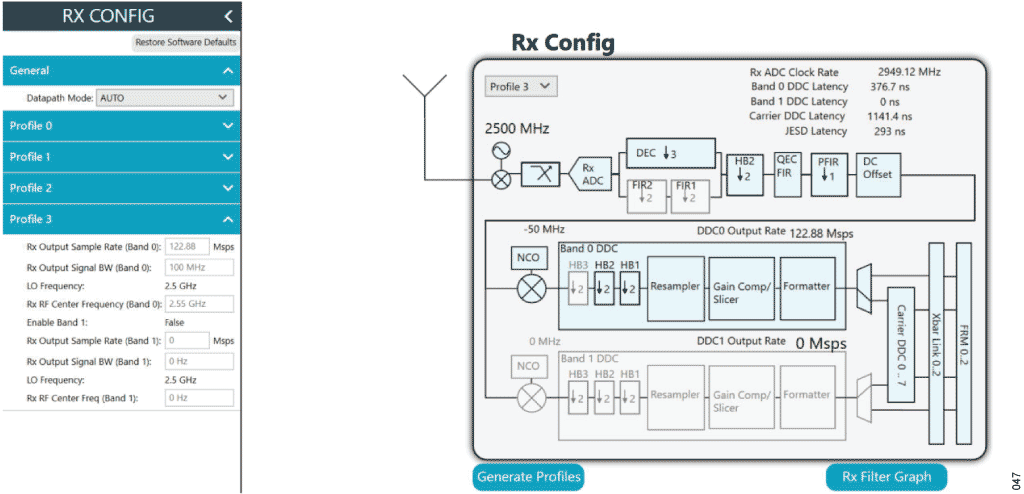
Ability to Configure 4 Different Profiles
Although the transceiver supports dual LO with required dividers, wide bandwidth support for transmitter, receiver, and observation receiver channels, the user must be able to configure them independently, which is allowed by using profiles. The maximum number of profiles supported by the transceiver is 4, which means the user can configure 4 x2T2R band combinations.
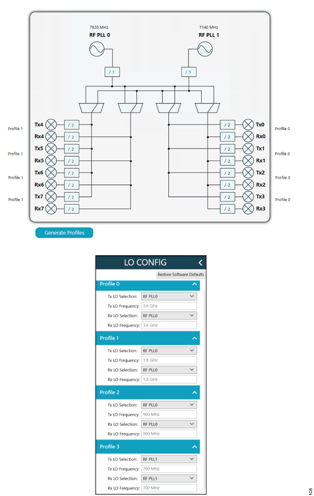
Figure 8 is a snippet of the GUI where in LO0 is assigned for Profile 0 and LO1 is assigned for Profile 1.
Another example of ability to assign RF PLL0 to 3.6GHz for Profile 0, 1.8GHz for Profile 1 and 900MHz for Profle 2, and RFPLL1 for 700MHz Band is also shown in the right side snippet in Figure 8.

Likewise, along with LO assignment for the profiles, each profile can be configured with required carrier frequencies, time division duplex (TDD) or frequency division duplex (FDD) mode, crest factor reduction (CFR)/DPD are enabled or not.
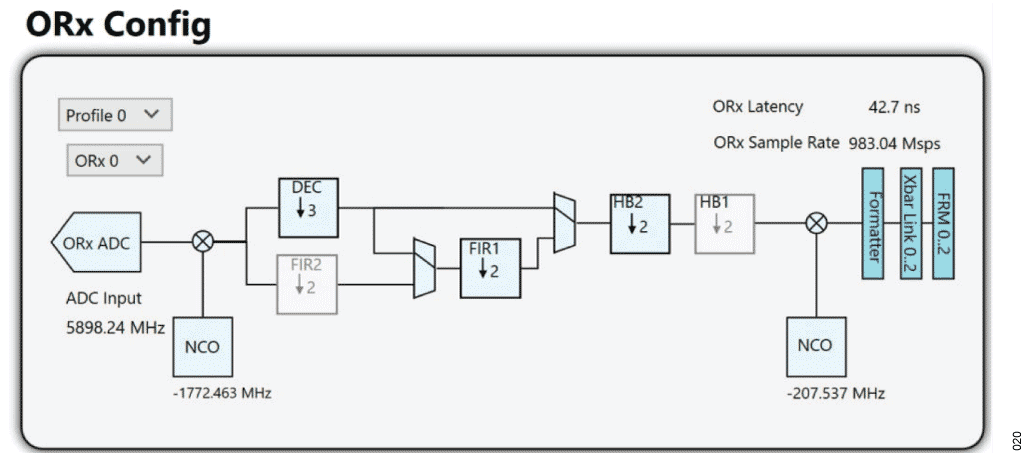
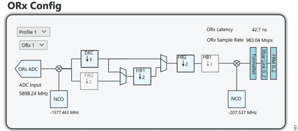
The observation receiver channels also have the profile assignment configuration capability, which aligns with the transmitter profiles as required for the calibrations (LOL, DPD) to run.
Also, the transceiver can work in mixed radio control mode, which means few transmitter/receiver can be in application processor interface (API) mode or other transmitter/receiver can be in PIN mode. This is required as TDD mode generally needs PIN mode for better time alignment while FDD mode can work in both API andpin radio control modes.
Multiband Possible Options
There may be many possible options to configure the required multibands, depending on the DL/UL frequencies of the bands. The main challenge comes from the LO frequency planning. Considering the duplex spacing, instantaneous bandwidth (IBW), and OBW of the bands to be supported, the user can select one of the following options:
- Option 1: Check possibility of having single LO for all bands that are to be supported.
- Option 2: Use single LO for DL bands of all bands, another LO for UL bands of all bands.
- Option 3: Use single LO for DL/ UL of same band. Careful placement of LO is required in this case.
- Option 4: Combine all the bands UL/DL frequencies so the 2 LOs can be accommodated.
Criterion for Frequency Planning for Multiband Operation
The user has the option to select any of the options as specified in section. However, the following must be considered while selecting the LO frequencies as the primary BW and synthesis BW are defined with respect to the LO frequencies.
- Make sure that the tracking calibrations such as quadrature error correction (QEC), LOL, and DPD run as expected
- For good DPD performance, at least 3x intermodulation distortion (IMD) products must be covered in the synthesis BW
- Make sure that the DL image does not fall on the wanted UL band and thereby no desensitization happens
- If using both LOs, make sure that they are separated by at least 100 MHz (applicable in case of carrier BW >=100M Hz)
Possible Combinations
The following multiband combinations are possible using ADRV9040 transceiver.
- 2x4T4R1O in FDD mode
- 2x 4T4R1O in TDD mode
- 1x4T4R1O FDD + 1x4T4R1O TDD
- 4x 2T2R Quad band in FDD mode
- 4x 2T2R Quad band in TDD mode
Example Multiband Solutions
Dual Band B1 (FDD) and B3 (FDD) 2X 4T4R Solution
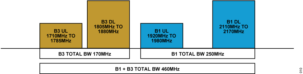
Both B1 and B3 are FDD bands and Table 2 shows the DL and UL band frequencies.
| Band | Uplink | Downlink |
| Band 1 | 1920-1980 | 2110-2170 |
| Band 3 | 1710-1785 | 1805-1880 |
Figure 9 shows the frequency bands placement. Band1 total BW including both UL and DL bands is 250MHz, while Band3 total BW including its UL and DL bands is 170MHz. The bandwidth required for both bands is 460MHz.
Considering the total BW of 460MHz needed for both bands, if the user needs to use a single LO for both the bands, a CDUC/CDDC enabled UC can be considered. Note that CDUC/CDDC bypassed case can not help here due to the maximum BW of 400MHz using 491.52MSPS rate. Also, it is not practical to use 491.52MSPS IQ rate for such a low BW signal (maximum carrier BW of 20MHz).
The user can also select one LO for DL/UL of Band1 and another LO for DL/UL of Band3 and using NCOs in the transmitter and receiver paths, it is possible to get to the appropriate carrier frequencies.


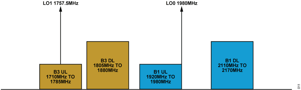
Band 1 Frequency Planning
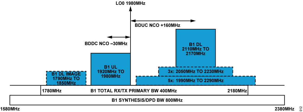
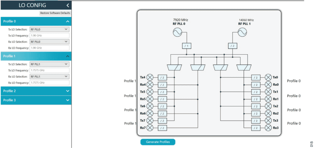
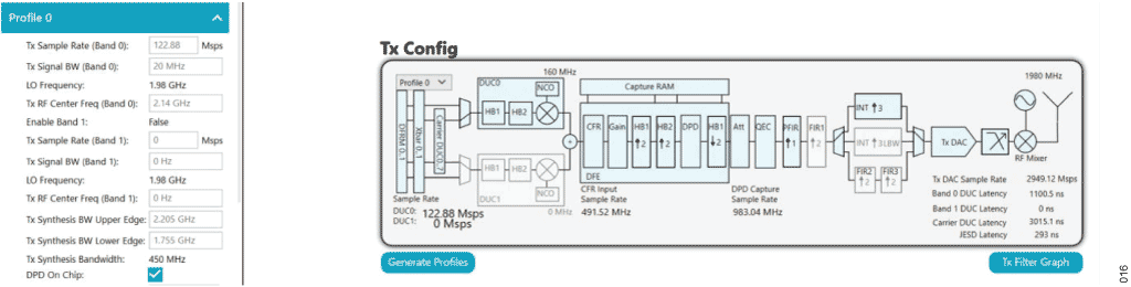
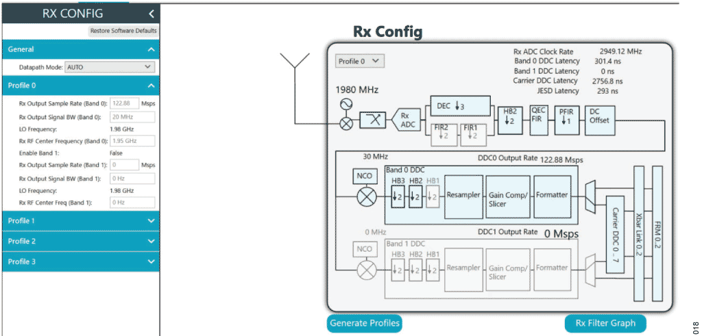
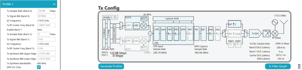
As shown in Figure 11, using LO0 of 1980MHz, to get to the DL center frequency of 2140MHz, BDUC NCO shift of 160MHz is used and to get to the UL center frequency of 1950MHz, BDDC NCO shift of −30MHz is used.

Band 3 Frequency Planning
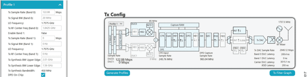
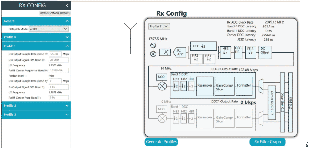
As shown in Figure 12, using LO1 of 1757.5MHz to get to the DL center frequency of 1842.5MHz, BDUC NCO shift of 85MHz is used and to get to the UL center frequency of 1742.5MHz, BDDC NCO shift of −10MHz is used.

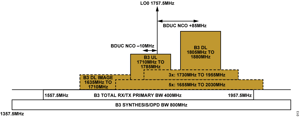
From the above Figure 11 and Figure 12, the following can be noted:
- The wanted signal is within the primary BW of 400MHz
- DL image is falling within 400MHz BW which means the QEC performancehas no impact
- DL signal 5x IMD products are falling with in 800MHz of synthesis BW
- DL image is not falling on the UL band which means no receiver desensitization is expected
- There is LO spacing of 222.5MHz
Transceiver Configuration for B1/B3
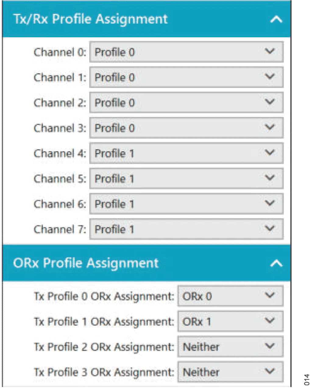
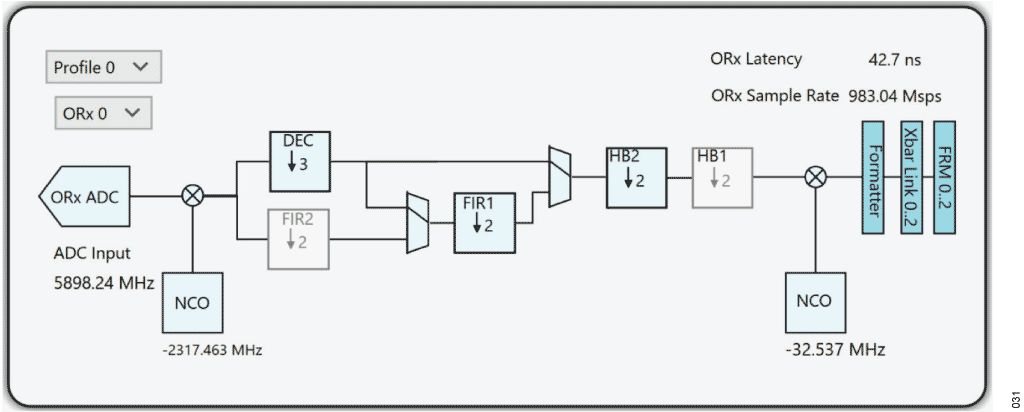
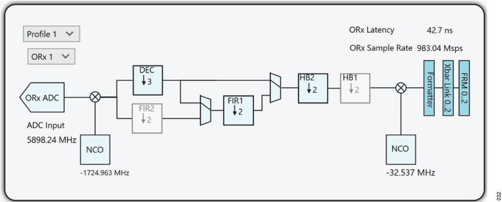
As there are 2 bands, user can assign 2 profiles, one profile for Band1 and another profile for Band3. As shown Figure 13, Tx0 to Tx3 and Rx0 to Rx3 are assigned for profile0 for Band1, TX4 to Tx7, and Rx4 to Rx7 are assigned for Profile1 for Band3. ORX0 has been assigned to Profile0 and ORX1 has been assigned to Profile1.


Dual Band B3 (FDD) and B40 (TDD) 2X 4T4R Solution
Band B3 is FDD and B40 is TDD band and Table 3 shows the DL and UL frequencies.
| Band | Uplink | Downlink |
| Band 3 (FDD) | 1710-1785 | 1805-1880 |
| Band 40 (TDD) | 2300-2400 | 2300-2400 |
Figure 21 for frequency bands placement, Band3 total BW including UL and DL bands is 170MHz and Band40 total BW including its UL and DL bands is 100MHz. The BW combining both the bands required is 690MHz.

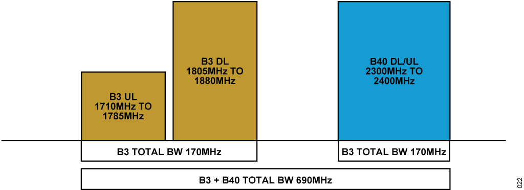
Considering the total BW of 690MHz needed for both bands, if the user needs to use a single LO, both CDUC/CDDC enabled and disabled use cases are not be feasible.
In this scenario, the user can also select one LO for DL/UL of Band3 and another LO for DL/UL of Band40 and using NCOs in the transmitter and receiver paths, it is possible to get to the appropriate carrier frequencies.
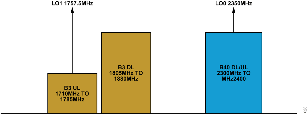
As shown in Figure 22, LO0 of 2350MHz is considered for Band40 DL/ UL paths and LO1 of 1757.5MHz is considered for Band3 DL/UL paths. LO0 of 2350MHz is considered such that no NCO shifts are required. LO1 frequency is selected such that the DL image does not fall on the UL band.

Band 3 Frequency Planning
Band 3 frequency planning remains same as explained Band 3 Frequency Planning.
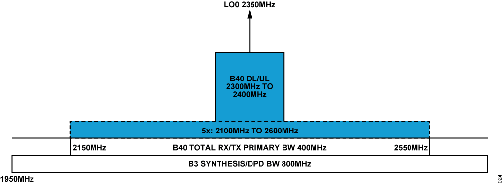
Band 40 Frequency Planning
Refer to Figure 23, since B40 is TDD, either transmitter or receiver path is on at any given time and there are no challenges here. LO frequency of center of the band, 2350MHz is chosen. The user can select any LO frequency, but NCO shifts may need to be used accordingly.
Note that 800MHz of synthesis BW is used here in this configuration which is not necessary and 500MHz would be fine.

From the frequency planning of both B3 and B40 bands, the following can be noted:
- The wanted signal is within the primary BW of 400MHz
- DL image is falling with in 400MHz BW which means the QEC performance has no impact
- DL signal 5x IMD products are falling with in 800MHz of synthesis BW
- In case of FDD band B3, DL image is not falling on the UL band which means no receiver desensitization is expected
- There is LO spacing of 592.5MHz between both LOs
Transceiver Configuration for B3/B40
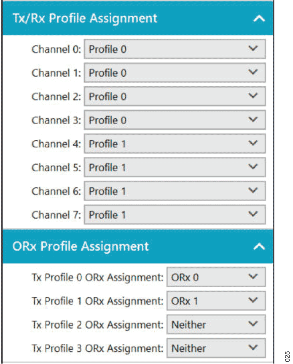
As there are 2 Bands, user can assign 2 Profiles- one profile for Band3 and another profile for Band40. As shown in the Figure 24, Tx0 to Tx3 & Rx0 to Rx3 are assigned for profile0 for Band40 and TX4 to Tx7 & Rx4 to Rx7 are assigned for Profile1 for Band3. ORX0 has been assigned for Profile0 and ORX1 has been assigned for Profile1.


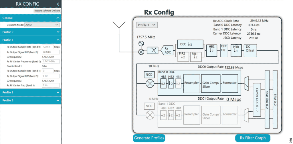
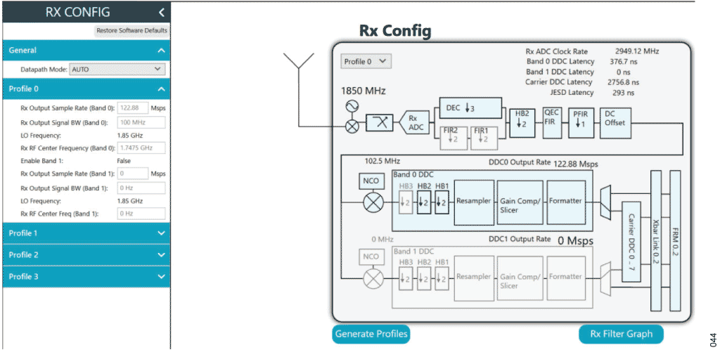
As shown in Figure 28, proceed with reciever configuration for Profile0- Band 1 after assigning the carrier center frequency in CDDC page.


Quad Band B3 (FDD), B40, B41, B78 4X 2T2R Solution
Band B3 is FDD and B40 is TDD band and Table 4 shows the DL and UL frequencies.
| Band | Uplink | Downlink |
| Band 3 (FDD) | 1710-1785 | 1805-1880 |
| Band 40 (TDD) | 2300-2400 | 2300-2400 |
| Band 41 (TDD) | 2496-2690 | 2496-2690 |
| Band 78 (TDD) | 3300-3800 | 3300-3800 |
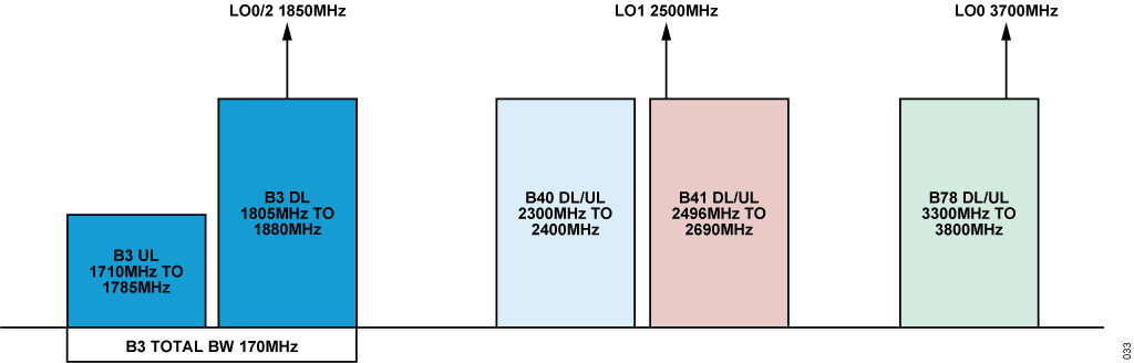
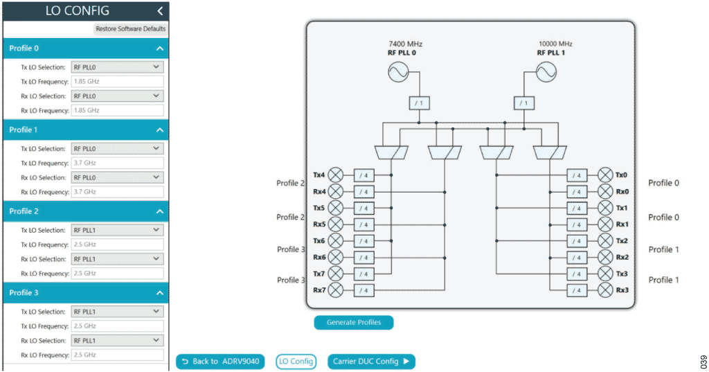
Figure 32 shows frequency bands placement, Band3 total BW including UL and DL bands is 170MHz for which user can select a single LO. Considering B78 Frequency band, one LO can be placed at 3700MHz (LO0), and LO0/2 can be used for B3 which is 1850MHz. For Bands B40 and B41, another LO, LO1 can be placed at 2500MHz which can cover both the bands.

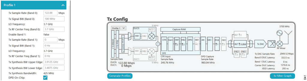
Band 78 Frequency Planning
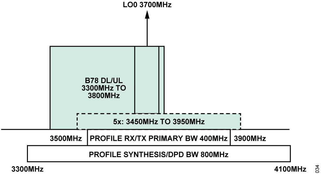
Figure 33 LO frequency of 3700 MHz is chosen assuming the carrier is placed at 3700MHz out of the full B78 band. Having LO at 3700MHz can cover the carriers placed from 3500MHz to 3800MHz which fall within primary BW of the profile. To cover the rest of the B78 band- 3300MHz to 3500MHz, LO change is required.

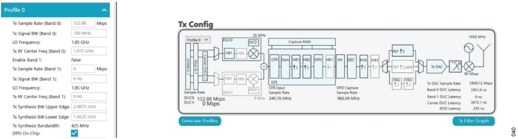
Band 3 Frequency Planning
As shown in Figure 34, using LO0/2 of 1850MHz (LO0 is used for B78), to get to the DL center frequency of 1842.5MHz, BDUC NCO+ CDUC NCO shift of -7.5MHz is used and to get to the UL center frequency of 1742.5MHz, BDDC NCO shift of -102.5MHz is used.

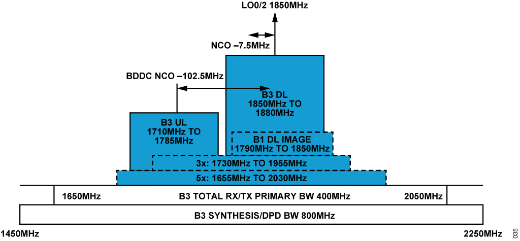
From the frequency planning of B3 band, the following can be noted:
- The wanted signal is within the primary BW of 400MHz
- DL image is falling with in 400MHz BW which means the QEC performance has no impact
- DL signal 5x IMD products are falling with in 800MHz of Synthesis BW
- DL image is not falling on the UL band which means no RX desensitization is expected
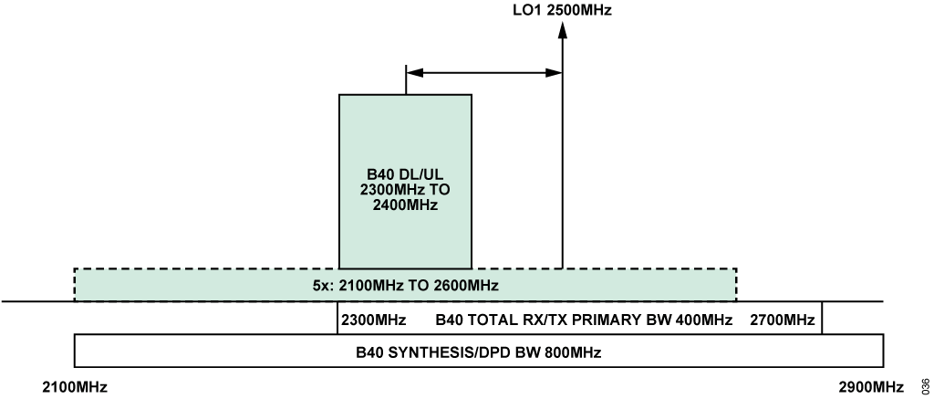
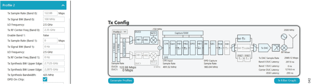
Band 40 Frequency Planning
As shown in Figure 35, using LO1 of 2500MHz, to get to the DL/UL center frequency of 2350MHz, BDUC/BDDC NCO shift of -150MHz is used. The carrier is assumed to be 100MHz placed at the center of the band.

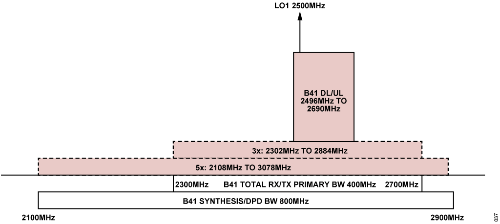
Band 41 Frequency Planning
As shown in Figure 36, using LO1 of 2500MHz, to get to the DL/UL center frequency of 2550MHz, BDUC/BDDC NCO shift of +50MHz is used. The carrier is assumed to be 100MHz placed at 2550MHz in the band.
Band 41 full RF bandwidth is 194MHz. Assuming the full BW needs to be covered without the LO change, only 3x IMD can be covered within 800MHz of synthesis BW. In this case, DPD correction may need to be tested thoroughly although it might meet.
The present example shows carrier placed at 2550MHz with 100MHz BW, whose 5xIMD products are covered with in the profile synthesis BW and it is expected that DPD performance is fine.

Transceiver Configuration for B3/B40/B41/B78
As there are 4 Bands, user can assign 4 profiles with each profile supporting each band for 2T2R configuration. As shown in Figure 37, Tx0/Tx1 and Rx0/Rx1 are assigned for Profile 0 for B3; Tx2/Tx3 & Rx2/Rx3 are assigned for profile1 for Band78; Tx4/Tx5 and Rx4/Rx5 are assigned for profile2 for Band40 and Tx6/Tx7 and Rx6/Rx7 are assigned for profile3 for Band41. Profile 0 and Profile 1 uses ORX0, while Profile 2 and Profile 3 uses ORX1.

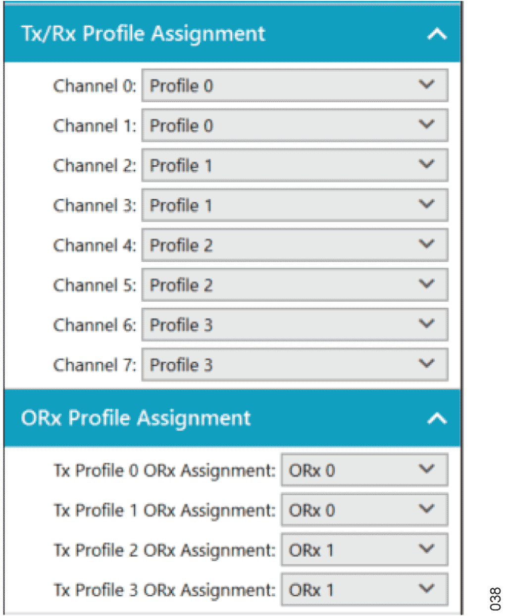


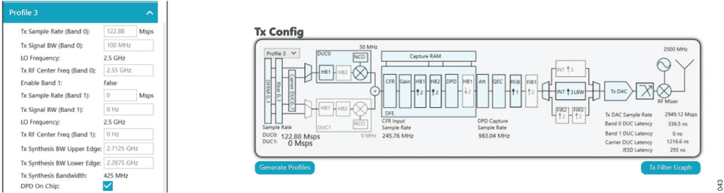
As shown in Figure 40, proceed with transmitter configuration for Profile1- Band 78 after assigning the carrier center frequency in CDUC page.


Few Notes
- By default, all the profiles available in GUI are TDD. If a profile has a FDD operation, is_TDD parameter flag must be set to false in JSON manually for the DPD to run in FDD.
- It is always recommended to test for the performance specifically QEC, LOL, and DPD with EVB on the customized UC that is targeted for multiband.
- Contact ADI EZONE for specific use case requests on multiband applications.