ADRV9040

RECOMMENDED FOR NEW DESIGNS

8T8R SoC with DFE, 400 MHz iBW RF Transceiver

Viewing:

Overview

  • Eight differential transmitters (Tx)
  • Eight differential receivers (Rx)
  • Two differential observation receivers (ORx)
  • Tunable range: 600 MHz to 6000 MHz
  • Single-band and Multiband (N x 2T2R/4T4R) capability
  • Four individual band profiles within tunable range (band profiles define bandwidth and aggregate sampling rate of a channel)
  • ADRV9040BBPZ-WB supports DPD for 400 MHz iBW/OBW
  • Simplifying system thermal solution
    • 13 W power consumption for all blocks enabled (use case is TDD 200 MHz instantaneous bandwidth and 200 MHz occupied bandwidth, with all blocks (DPD, CFR, and CDUC/CDDC) enabled)
    • 125°C maximum junction temperature for intermittent operation, 110°C for continuous (operating lifetime impact at >110°C can be offset by operation at <110°C based on acceleration factors)
  • Fully integrated DFE (DPD, CDUC, CDDC, and CFR) engine that reduces FPGA resources and halves SERDES lane rate
    • DPD adaptation engine for power amplifier linearization
    • CDUC/CDDC—maximum eight component carriers (CCs) per each transmitter/receiver channel
  • Multistage CFR engine
  • Supports DTx (micro sleep) power saving mode in downlink
  • Supports JESD204B and JESD204C digital interface
  • Multichip phase synchronization for all local oscillator (LO) and baseband clocks
  • Dual fully integrated fractional-N RF synthesizers
  • Fully integrated clock synthesizer

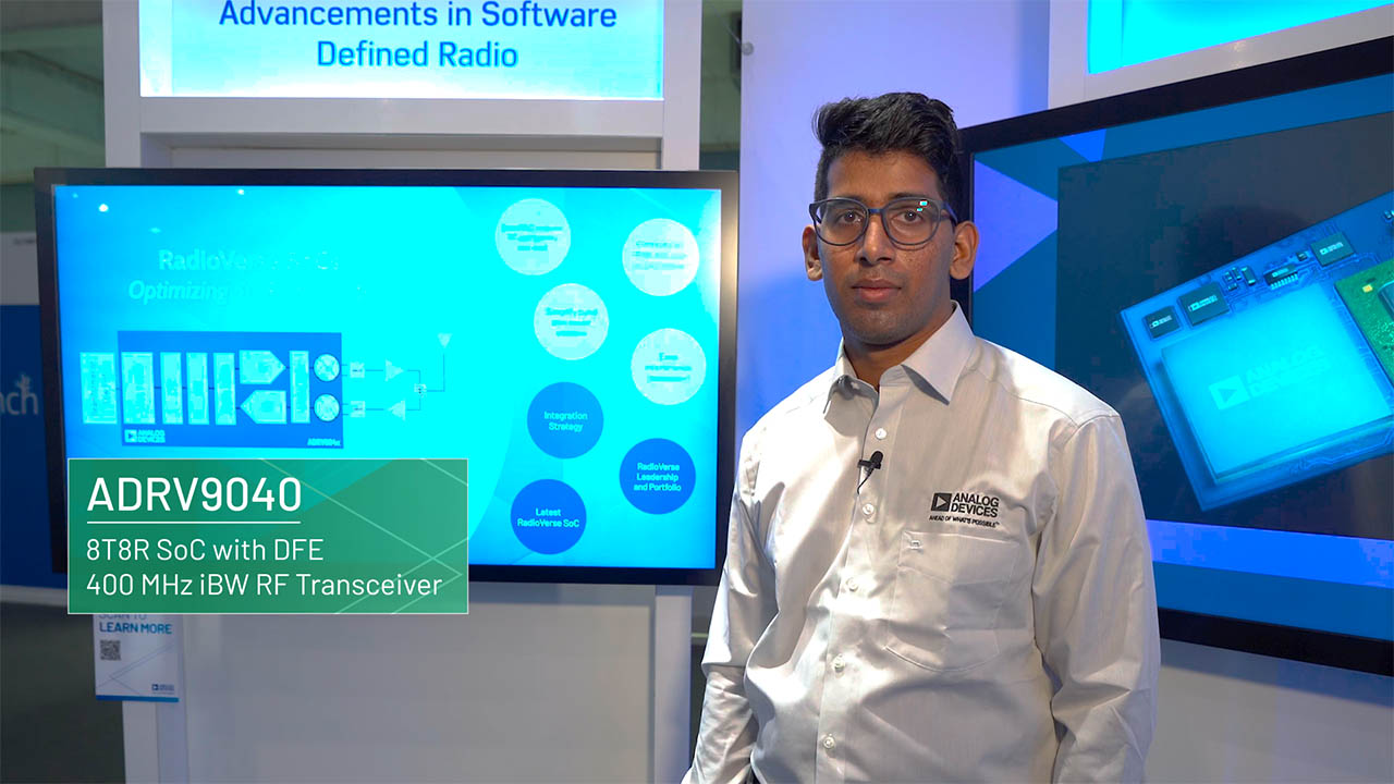
The ADRV9040 is a highly integrated, system on chip (SoC) radio frequency (RF) agile transceiver with integrated digital front end (DFE). The SoC contains eight transmitters, two observation receivers to monitor transmitter channels, eight receivers, integrated LO and clock synthesizers, and digital signal processing functions. The SoC meets the high radio performance and low power consumption demanded by cellular infrastructure applications including small cell base-station radios, macro 3G/4G/5G systems, and massive MIMO base stations.

The receiver and transmitter signal paths use a zero-IF (ZIF) architecture that provides wide bandwidth with dynamic range suitable for contiguous and non-contiguous multi-carrier base-station applications. The ZIF architecture has the benefits of low power plus RF frequency and bandwidth agility. The lack of aliases and out-of-band images eliminate anti-aliasing and image filters. This reduces both system size and cost, also making band independent solutions possible.

The device also includes two wide-bandwidth observation path receiver subsystems to monitor transmitter outputs. This SoC subsystem includes automatic and manual attenuation control, DC offset correction, quadrature error correction (QEC), and digital filtering. GPIOs that provide an array of digital control options are also integrated.

Multi-band capability is enabled by additional LO dividers and wideband operation. This allows four individuals band profiles within the tunable range, so maximizing use case flexibility.

The SoC has fully integrated DFE functionality, which includes carrier digital up/down conversion (CDUC and CDDC), crest factor reduction (CFR), digital predistortion (DPD), closed-loop gain control (CLGC) and voltage standing wave ratio (VSWR) monitor.

The CDUC feature of the ADRV9040 filters and places individual component carriers within the band of interest. The CDDC feature, with its eight parallel paths, processes each carrier individually before sending over the serial data interface.

The CDUC and CDDC reduce serialization/deserialization (SERDES) interface data rates in non-contiguous carrier configurations. This integration also reduces power compared to an equivalent FPGA based implementation.

The CFR engine of the ADRV9040 reduces the peak-to-average ratio (PAR) of the input signal, which enables higher efficiency transmit line ups while reducing the processing load on baseband processors.

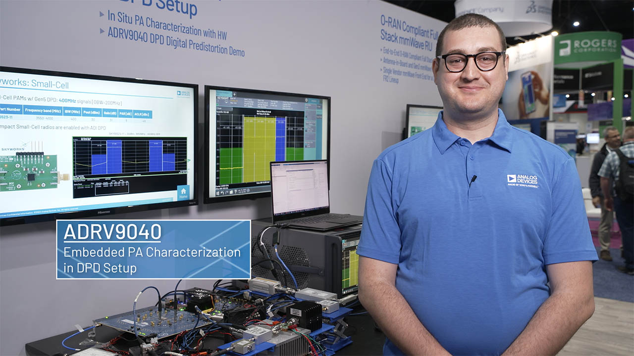
The SoC also contains a fully integrated DPD engine for use in power amplifier linearization. The DPD enables the high-efficiency power amplifiers, which reduce the power consumption of base-station radios and the number of SERDES lanes interfacing with baseband processors. The DPD engine incorporates a dedicated long-term DPD (LT-DPD) block, which provides the support for GaN power amplifiers. The ADRV9040 tackles charge-trapping property of GaN power amplifiers with its LT-DPD block, hence improving the emissions and error vector magnitude (EVM). The SoC includes an ARM Cortex-A55 quad core processor to independently serve DPD, CLGC, and VSWR monitor features. The dedicated processor, together with the DPD engine, provides industry leading DPD performance.

The serial data interface consists of eight serializer and deserializer lanes. The interface supports the JESD204C standards, and both fixed and floating-point data formats are supported. The floatingpoint format allows internal automatic gain control (AGC) to be transparent to the baseband processor.

The ADRV9040 is powered directly from 0.8 V, 1.0 V, and 1.8 V regulators and is controlled through a standard SPI serial port. The comprehensive power-down modes are included to minimize the power consumption in normal use. The device is packaged in a 27 mm × 20 mm, 736-ball grid array.

Applications

  • 3G/4G/5G time division duplex (TDD)/frequency division duplex (FDD) small cell, massive MIMO, and macro base stations

ADRV9040
8T8R SoC with DFE, 400 MHz iBW RF Transceiver
ADRV9040 Functional Block Diagram ADRV9040 Pin Configuration ADRV9040 Chip
Add to myAnalog

Add product to the Products section of myAnalog (to receive notifications), to an existing project or to a new project.

Create New Project
Ask a Question

Documentation

Learn More
Add to myAnalog

Add media to the Resources section of myAnalog, to an existing project or to a new project.

Create New Project

Software Resources

API Device Drivers 1

Device Application Programming Interface (API) C code drivers provided as reference code allows the user to quickly configure the product using high-level function calls. The library acts as an abstraction layer between the application and the hardware. The API is developed in C99 to ensure agnostic processor and operating system integration. Customers can port this application layer code to their embedded systems/ Baseband Processor by integrating their platform-specific code base to the API HAL layer. To request this software package, go to the Software Request Form signed in with your MyAnalog account and under “Target Technology option - select “Wireless Communications" and choose processor/SOC as "ADRV9040 or ADRV9044" , select the check box as well and submit the form. You will receive an email notification with a link for software download.


Hardware Ecosystem

Parts Product Life Cycle Description
Amplifier-Based Front Ends 2
ADRF5515A RECOMMENDED FOR NEW DESIGNS Dual-Channel, 3.3 GHz to 4.0 GHz, 20 W Receiver Front End
ADRF5515 RECOMMENDED FOR NEW DESIGNS

Dual-Channel, 3.3 GHz to 4.0 GHz, 20 W Receiver Front End

Clock ICs 2
AD9528 RECOMMENDED FOR NEW DESIGNS JESD204B/JESD204C Clock Generator with 14 LVDS/HSTL Outputs
AD9545 RECOMMENDED FOR NEW DESIGNS Quad Input, 10-Output, Dual DPLL/IEEE 1588, 1 pps Synchronizer and Jitter Cleaner
Low-Noise Amplifiers (LNAs) & Power Amplifiers 2
ADL5545 RECOMMENDED FOR NEW DESIGNS 30 MHz to 6 GHz RF/IF Gain Block
ADL5611 RECOMMENDED FOR NEW DESIGNS 30 MHz to 6 GHz RF/IF Gain Block
RF Switches 1
ADRF5250 RECOMMENDED FOR NEW DESIGNS 0.1 GHz to 6 GHz Silicon SP5T Switch
Switching Regulators & Controllers 2
ADP5056 RECOMMENDED FOR NEW DESIGNS Triple Buck Regulator Integrated Power Solution
LT8627SP RECOMMENDED FOR NEW DESIGNS 18V/16A Step-Down Silent Switcher 3 with Ultralow Noise Reference
Modal heading
Add to myAnalog

Add product to the Products section of myAnalog (to receive notifications), to an existing project or to a new project.

Create New Project

Tools & Simulations

ADIsimRF

ADIsimRF is an easy-to-use RF signal chain calculator. Cascaded gain, noise, distortion and power consumption can be calculated, plotted and exported for signal chains with up to 50 stages. ADIsimRF also includes an extensive data base of device models for ADI’s RF and mixed signal components.

Open Tool

SDR Integrated Transceiver Design Resources

This site contains the device documentation packages for the SDR Integrated Transceivers including user guides, IBIS models, and PCB files.

Open Tool

Evaluation Kits

eval board
ADS10-V1EBZ

ADS10-V1EBZ Evaluation Board

Features and Benefits

Xilinx Virtex Ultrascale+ XCVU35P-3FSHV2892E FPGA.

  • One (1) FMC+ connector.
  • Twenty (24) 32.75Gbps transceivers supported by one (1) FMC+ connector.
  • On-board HBM DRAM in FPGA.
  • Simple USB 3.0 port interface.

Product Details

When connected to a specified Analog Devices high speed converter evaluation board, the ADS10-V1EBZ works as a data capture/transmit board. Designed to support the highest speed JESD204B/C data converters, the FPGA on the ADS10-V1EBZ acts as the data receiver for high speed ADC's, and as the transmitter for high speed DAC's.

eval board
EVAL-ADRV904x

Product Details

INTRODUCTION

The ADRV904x family evaluation system enables customers to evaluate an ADRV904x device without having to develop custom hardware or software. The system is comprised of an ADRV904x customer evaluation (CE) board and an ADS10-V1EBZ motherboard with accompanying wall adapter power supplies for both. The evaluation software uses the Analysis, Control, Evaluation (ACE) software developed by Analog Devices, Inc., extended by an ADRV904x specific board plugin. This plugin can be run with ACE on a Windows host PC communicating with the ADS10-V1EBZ motherboard using Ethernet. The ADS10-V1EBZ functions as a baseband processor running an application (ADRV904x command server) for controlling and communicating with the ADRV904x device.

This document also serves as a quick startup guide for the ADRV904x configurator, which is built into the ADRV9040 board plugin for ACE. The ADRV904x configurator allows the user to explore various configurations of an ADRV904x device to arrive at a desired use case configuration. The ADRV904x configurator also provides an overview of the frequency responses of the receiver (Rx), transmitter (Tx), and the observation receiver (ORx) datapaths for a chosen configuration.

This user guide details the steps required to install the ADRV904x evaluation software, program an existing use case, and evaluate the ADRV904x transmitter, receiver, and observation receiver datapaths. The configurator sections of this user guide enable the user to generate a new use case and view its corresponding datapath configurations and filter graphs for the ADRV904x. Note that this document updates as the configurator development progresses and as additional functionalities are added to the tool.

ADS10-V1EBZ
ADS10-V1EBZ Evaluation Board
ADS10-V1EBZ - Top View ADS10-V1EBZ - Bottom View ADS10-V1EBZ - Angle View
EVAL-ADRV904x
EVAL-ADRV904x Board Photo Angle View EVAL-ADRV904x Board Photo Top View EVAL-ADRV904x Board Photo Bottom View

Latest Discussions

Recently Viewed