CN0190


Overview
Design Resources
Design & Integration File
- Schematic
- Bill of Materials
- Gerber Files
- PADS Files
- Assembly Drawing
Evaluation Hardware
Part Numbers with "Z" indicate RoHS Compliance. Boards checked are needed to evaluate this circuit.
- EVAL-CN0190-EB1Z ($86.14) Robust, Multivoltage, High Efficiency, 25 W Universal Power Supply Module with 6 V to 14 V Input
Features & Benefits
- 12 different voltage and current output conditions
- Configure the all other channels to be powered off
Product Categories
Markets and Technologies
-
- Body Temperature Measurement Solutions
- Therapy Device Solutions for Healthcare
- Ultrasound Solutions
- Digital X-Ray Solutions
- Wearable Health Monitor Solutions
- Insulin Pump Solutions
- Oxygen Saturation (SpO2) Measurement Solutions
- Respiration Rate Measurement Solutions
- Non-Invasive Blood Pressure (NIBP) Solutions
- Electrocardiogram (ECG) Measurement Solutions
Parts Used
Documentation & Resources
-
CN0190 Software User Guide10/18/2018WIKI
Circuit Function & Benefits
Modern complex systems using various combinations of FPGAs, CPUs, DSPs, and analog circuits typically require multiple voltage rails. In order to provide high reliability and stability, the power system must not only provide the multiple voltage rails but also include proper sequencing control and necessary protection circuits.


The module shown in Figure 1 is a reference solution for multivoltage power systems. The design can easily be adapted to customer requirements and provides the most popular system voltages. The circuit uses an optimum combination of switching and linear regulators to provide an overall efficiency of approximately 78% when the outputs are fully loaded. Output power delivered under full load is approximately 25 W.
Circuit Description
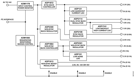
A functional block diagram of the circuit is shown in Figure 1. Complete schematics of each section are included in the CN0190 Design Support Package. This module supplies most of the typical power rails required for digital and analog circuits and also demonstrates an easy way to realize overvoltage, undervoltage, and overcurrent detection and protection. In addition, this module shows how to implement sequencing and power margining control.
The circuit is flexible and can accept a wide input voltage range from 6 V to 14 V. This is possible because the highly efficient switching controllers and regulators used in the first stage of each power rail have correspondingly wide input ranges. The ADM1178 block provides overvoltage and overcurrent detection and protection for the input supply, as well as hotswap control for the whole system. The ADM1066 offers a single-chip solution for power supply monitoring and sequencing control for all of the 12 power rails and also margining control for the 3.3V(2A) rail.

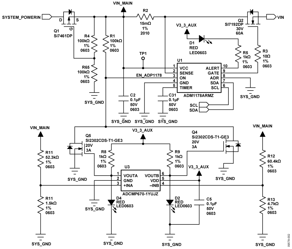
Description of Input Protection Circuits
The circuit shown in Figure 2 provides input protection for the module and is described in detail in the following sections.
Input Voltage Polarity Reversal Protection
Protection against input voltage reversal is provided by the P-channel MOSFET, Q1. In normal operation with positive input voltages, Q1 (SI7461DP) turns on when the voltage between SYSTEM_POWERIN and SYS_GND is positive and larger than the gate-to-source threshold voltage. If the input is negative (fault condition with polarity reversed), Q1 will turn off to prevent the main circuit from damage, and its function is similar to that of a diode.
Because of the high input current (up to 6.67 A), a P-channel MOSFET is much better than a diode because the low onresistance of the MOSFET minimizes power dissipation. For example, the on-resistance of the SI7461DP is approximately 0.02 Ω for a VGS of −4.5 V. A current of 6.67 A yields a power dissipation of only 0.9 W. A diode with 0.6 V forward drop would dissipate about 4 W at the same current. The maximum VGS of the SI7461DP is ±20 V which covers the module's input range of 6 V to 14 V. Note that the gate bias voltage for Q1 is supplied by the output of the divider R4-R5 to make Q1 robust to input voltage changes.
Overcurrent Detection and Protection
Input current is sensed by using the ADM1178 hot-swap controller/digital power monitor to measure the voltage drop across R2, the 15 mΩ current sense resistor. The ADM1178 internal FET drive controller regulates the maximum load current by modulating the gate voltage of the N-channel MOSFET, Q2. When the voltage through the sense resistor is more 100 mV, the gate drive voltage limits the current through Q2, thereby protecting downstream circuitry.
Overvoltage and Undervoltage Detection and Protection
The ADCMP670-1 is a dual, low power, high accuracy comparator with an internal 400 mV reference. The two comparators and the external MOSFETs, Q4 and Q5, are configured as a window comparator. The low and high voltage thresholds of 5.54 V and 14.35 V, respectively, are set by the dividers R10–R11 and R12–R13. If the input voltage is outside the window on the high side, VOUTA goes high, Q5 turns on, and the ON pin of the ADM1178 is pulled low, thereby turning Q2 off. Similarly, if the input voltage is outside the window on the low side, VOUTB goes high, Q4 turns on, and the ON pin of the ADM1178 is pulled low, thereby turning Q2 off.
Overcurrent, Undervoltage Overvoltage Calculation Summary
Overcurrent Threshold = 100 mV ÷ 15 mΩ = 6.67 A
Power in Current Sense Resistor = 100 mV × 6.67 A = 0.667 W (use 0.75 W resistor)
High Voltage Threshold = 0.4 V(R10 + R11)/R11 = 14.35 V
Low Voltage Threshold = 0.4 V(R12 + R13)/R11 = 5.54 V
IC Protection Technology
There are also several protection features associated with the individual power ICs. Undervoltage lockout (UVLO) disables all inputs and the output to an IC when the input voltage is less than the minimum voltage required for the rails to behave in a predictable manner during power-up. Thermal shut down (TSD) prevents the IC from damage due to high operating junction temperature. Overcurrent protection (OCP) also protects the IC when there is a short on the output. Further details can be found on the individual power IC data sheets.
Description of Power Rails in Universal Power Supply Module
There are 12 power rails supplied by this module summarized in Table 1. The following four rails are based on the synchronous buck topology: 3.3V(2A), 1.5V(1A), 1.8V(1A), 1.2V(0.5A). The following two rails are based on the nonsynchronous buck topology: 5.0V(1A), 2.5V(1A). The −5 V rail is generated from the +5.0V(1A) rail using the inverting buck-boost topology. The positive and negative analog rails {Px,Nx}(0.1A) are generated by the Sepic-Cuk topology. The last three rails are supplied by LDOs. Each rail has an independent power on LED indicator.
Table 1 lists the voltage, maximum current capability, key features of the power IC, and typical applications for each power rail.
| Output Voltage | Current | Power IC | General Description of Power IC | Typical Applications |
| 3.3 V | 2 A | ADP1872 | The ADP1872 is a versatile current-mode, synchronous step-down controller that provides superior transient response, optimal stability, and current limit protection by using a constant on-time, pseudo-fixed frequency with a programmable current-sense gain, current-control scheme. | General purpose digital circuits, I/O voltages |
| 5.0 V | 1 A | ADP1864 | The ADP1864 is a compact, inexpensive, constant-frequency, current-mode, step-down dc-to-dc controller. The ADP1864 drives a P-channel MOSFET that regulates an output voltage as low as 0.8 V with ±1.25% accuracy, for up to 5 A load currents, from input voltages as high as 14 V. The device can operate at 100% duty cycle for low dropout voltage. | |
| 1.5 V | 1 A | ADP2114 | The ADP2114 is a versatile, synchronous, dual, step-down switching regulator that satisfies a wide range of customer point-of-load requirements. The two PWM channels can be configured to deliver independent outputs at 2A and 2A (or 3 A/1 A) or can be configured as a single interleaved output capable of delivering 4A. The two PWM channels are 180° phase shifted to reduce input ripple current and to reduce input capacitance. | Core voltage of the MCU, DSP, or FPGA |
| 1.8 V | 1 A | |||
| 2.5 V | 1 A | ADP2300 | The ADP2300 is a compact, constant-frequency, current-mode, step-down dc-to-dc regulator with integrated power MOSFET. ADP2300 operates from input voltages of 3.0 V to 20 V, making it suitable for a wide range of applications. | |
| 1.2 V | 0.5 A | ADP2108 | The ADP2108 is a high efficiency, low quiescent current step-down dc-to-dc converter. The total solution requires only three small external components. It uses a proprietary, high-speed current mode, constant frequency PWM control scheme for excellent stability and transient response. Operation at 100% duty cycle gives low dropout voltage. | |
| 1.0 V | 2A | ADP1741 | The ADP1741 is a low dropout (LDO) CMOS linear regulator that operates from 1.6 V to 3.6 V and provide up to 2A of output current. | |
| Px | 0.1 A | ADP1613 | The ADP1613 are step-up dc-to-dc switching converters with an integrated power switch capable of providing an output voltage as high as 20 V. | Analog or mixed-signal systems such as ADC, DAC, amplifiers, analog multiplexers |
| Nx | 0.1 A | |||
| 3.3 V | 0.15 A | ADP151 | The ADP151 is an ultralow noise (9µV), low dropout, linear regulator that operates from 2.2V to 5.5V and provides up to 200 mA of output current. | |
| 3 V | 0.1 A | ADP121 | The ADP121 is a quiescent current, low dropout, linear regulator that operates from 2.3V to 5.5V and provides up to 150 mA of output current. | |
| −5 V | 0.2 A | ADP2301 | The ADP2301 is compact, constant-frequency, current-mode, step-down dc-to-dc regulator with integrated power MOSFET. The ADP2301 devices operate from input voltages of 3.0 V to 20 V, making them suitable for a wide range applications. |
Low dropout linear regulators (LDOs) are generally easier to use than switching power and have lower noise and better transient response characteristics. However, they have low efficiency when the output voltage is much less than the input voltage. This limits their current output capability.
A switching power supply is usually the best choice for the first stage of the power system because of its high efficiency and high current output. The noise caused by switching supplies can be minimized by properly designing the control loop and using good PCB layout techniques. If care is taken, switching supplies can often be used to power high performance analog circuits as described in the following circuit notes: CN-0135, CN-0137, CN-0141, and CN-0193.
| VOUT | VIN(MIN) | VIN(MAX) | IOUT(MAX) | IRIPPLE | VRIPPLE | ISTEP | VSTEP |
| 3.3V(2A) | 6 V | 14 V | 4 A | 33% IOUT(MAX) | 1% VOUT | 80% IOUT(MAX) | 5% VOUT |
| 5.0V(1A) | 6 V | 14 V | 2 A | 33% IOUT(MAX) | 1% VOUT | 75% IOUT(MAX) | 5% VOUT |
| 2.5V(1A) | 6 V | 14 V | 1 A | 33% IOUT(MAX) | 1% VOUT | 80% IOUT(MAX) | 5% VOUT |
| {Px,Nx}(0.1A) | 6 V | 14 V | 0.1 A | 33% IOUT(MAX) | 1% VOUT | 70% IOUT(MAX) | 5% VOUT |
| 1.8V(1A) | 3.2 V | 3.4 V | 3 A | 33% IOUT(MAX) | 1% VOUT | 90% IOUT(MAX) | 5% VOUT |
| 1.5V(1A) | 3.2 V | 3.4 V | 1 A | 33% IOUT(MAX) | 1% VOUT | 90% IOUT(MAX) | 5% VOUT |
| 1.2V(0.5A) | 3.2 V | 3.4 V | 0.5 A | 33% IOUT(MAX) | 1% VOUT | 90% IOUT(MAX) | 3% VOUT |
Individual Switching Supply Designs Using ADIsimPower
ADIsimPower is and interactive design tool that both simplifies the power IC selection process and provides the information required to build an optimized linear or dc-todc converter. The program performs all the tedious calculations and provides a final schematic, recommended bill-of-materials, and predicted performance. The component recommendations come from a large database of parts with known electrical characteristics. The user simply provides the system-level inputs to the program; such as minimum input voltage, maximum input voltage, output voltage, output current, output current ripple, output voltage ripple, transient response, etc., as shown in Table 2.
All the power rails in this power module based on switching controllers and regulators are designed using ADIsimPower except the −5V(0.2A) rail using ADP2301, which is based on inverting buck-boost topology.
See more details about ADIsimPower in the article “ADIsimPowerM Provides Robust, Customizable DC-to-DC Converter Designs” and at www.analog.com/ADIsimPower.
Design Example 1. 3.3V(2A)Rail Using the ADP1872
Figure 3 shows the circuit schematic of the synchronous buck topology controlled by the ADP1872. This circuit can be divided into three parts. Part A generates the bias voltage for ADP1872, part B is the enable control, and part C is switching regulator part of the rail.
The ADP1872 operates on a wide range of bias voltages from 2.75 V to 5.5 V. In this circuit the bias voltage is supplied by a 4.7 V Zener diode combined with an NPN buffer transistor as shown in Part A of Figure 3. The Zener diode selected (DDZ9687) has a Zener voltage of 4.7 V at 50 μA current. The ADP1872 can accept an input voltage as high as 20 V.
Pin 2 (COMP/EN) of the ADP1872 not only connects to the internal precision enable circuitry but also to the output of the internal error amplifier that controls the overall loop characteristic. The N-channel MOSFET, Q9, is used to ground the enable control of the ADP1872, thereby disabling the device. When Q9 is off, and the ADP1872 is enabled, the loop characteristic is controlled by the C11, C12, and R16 network. Q8 acts as an inverter so that a positive logic signal to the input of Part B (EN_3.3V) enables the ADP1872.
The design shown in Part C of Figure 3 was generated using ADIsimPower with the inputs shown in Table 2.


Design Example 2. Positive and Negative Analog Rails {Px,Nx}(0.1A) with Overcurrent Detection and Protection for Output
The positive and negative analog rails, {Px,Nx}(0.1A), are designed using the ADP1613 step-up controller based on Sepic-Cuk topology. The output can be set to four different symmetrical output voltages by changing the value of resistors in the feedback path. The voltages can be set to {+2.5V,−2.5V}, {+5V,−5V}, {+12V,−12V}, and {+15V,−15V}. Figure 4 shows the circuit where all components were selected based on ADIsimPower. The output capacitors were increased to 10 μF to further reduce the output ripple on the analog supplies. Also an external LC filter using a ferrite bead and a 3T capacitor is used for noise suppression. R76 and R77 are 240 mΩ shunt resistors added for overcurrent detection and do not significantly affect the characteristics of the control loop.
The overcurrent detection circuit is shown in Figure 5. The ADM1170 is a hot-swap controller with soft start and is used for overcurrent detection for the positive output rail in this circuit. The internal overcurrent detection circuit accepts a voltage from 1.6 V to 16.5 V which includes the {Px,Nx} output ranges from 2.5 V to 15 V. When the voltage between SENSE+ and SENSE− is larger than 50 mV(typical), the gate pin is grounded, which shuts down the ADP1613. The overcurrent threshold is set to 208 mA (typical) by the 240 mΩ shunt resistor, R76.


The overcurrent detection circuit for the negative output rail uses the AD628 high common-mode voltage, programmable gain difference amplifier combined with ADCMP350 comparator with on-chip 0.6 V reference. The AD628 is a two-stage amplifier. The first stage is a difference amplifier with a fixed gain of 0.1. The gain of the second stage, G, can be programmed by external resistors. The overcurrent threshold and shunt resistor are the same values as used on the positive rails. The gain of second stage amplifier is G = 125, which is calculated from Equation 1 by solving for G:

where ITHRESHOLD = 208 mA, and RSHUNT = 240 mΩ.
Because the AD628 is powered by the {Px,Nx} rails, both rails need time to settle during the module’s initial power-on interval. During this time, the AD628 may work abnormally due to the undefined power supply levels. The 2 kΩ resistor, R62, is used to pull down the output of AD628 before the {Px,Nx} rails are at their final value, thereby preventing the circuit from going into a latch-up condition.
Design Example 3. −5V(0.2A) Using Inverting Buck-Boost Topology Controlled by the ADP2301
ADP2301 is nonsynchronous step-down regulator. In the circuit shown in Figure 6 it is used in the inverting buckboost topology to generate a negative voltage. This circuit is not directly supported in ADIsimPower, but is described in detail in Application Note AN-1083, "Designing an Inverting Buck Boost Using the ADP2300 and ADP2301 Switching Regulators." In this topology the VIN pin and GND pin of the ADP2301 are connected to the input and output of the rail, respectively. Other negative voltages can be generated by changing the value of the feedback resistors. However, it is important to make sure that |VIN| + |VOUT| is less than the maximum 20 V input voltage of ADP2301.


Power Supply Monitoring, Sequencing, and Margining Control
Voltage Monitoring
The ADM1066 Super Sequencer® is a configurable device that offers a single-chip solution for supply monitoring and sequencing in multiple-supply systems. The circuit is shown in Figure 7. The system input power is connected to VH of the ADM1066. All the power rails except −5V(0.2A) connect to VPx, VXx and AUXx directly after attenuation by the resistor divider. See AN-780 and AN-782 for more details about how to monitor high voltage or negative inputs.
The ADM1066 has up to 10 supply fault detectors (SFDs). The inputs can be configured to detect an undervoltage fault (the input voltage drops below a preprogrammed value), an overvoltage fault (the input voltage rises above a preprogrammed value), or an out-of-window fault (the input voltage is outside a preprogrammed range). All the power supplies in the module are monitored using the out-ofwindow fault criterion. The thresholds of each window are set to VOUT + 5% and VOUT − 5%. The parameters for each supply are listed in Table 3.
The 10 PDO outputs of the ADM1066 control all the 12 power rails. The 5.0V(1A), −5V(0.2A), and {Px,Nx}(0.1A) share a single PDO pin. All the other rails are controlled by individual PDO pins.


| Power Rail | VMAX (V) | VMAX (V) | Resistor Divider | Overvoltage Threshold (V) | Undervoltage Threshold (V) | |
| VX1 | 1.0V_2A | 1.05 | 0.95 | 1 | 1.05 | 0.95 |
| VX2 | 1.5V_1A | 1.575 | 1.425 | 5/6 | 1.31 | 1.19 |
| VX3 | 1.2V_0.5A | 1.26 | 1.14 | 1 | 1.26 | 1.14 |
| VX4 | 3.3V_0.1A | 3.465 | 3.135 | 5/16 | 1.08 | 0.98 |
| VX5 | 1.8V_1A | 1.89 | 1.71 | 11/16 | 1.30 | 1.18 |
| VP1 | 5.0V_1A | 5.25 | 4.75 | 1 | 5.25 | 4.75 |
| VP2 | 3.3V_2A | 3.465 | 3.135 | 1 | 3.465 | 3.135 |
| VP3 | 2.5V_1A | 2.625 | 2.375 | 1 | 2.625 | 2.375 |
| VP4 | 3.0V_0.1A | 3.15 | 2.85 | 1 | 3.15 | 2.85 |
| VH | VIN | 14.20 | 5.70 | 1 | 14.20 | 5.70 |
| AUX1 | Nx_0.1A | −2.375 | −2.375 | 1/11 | 1.65 | 0.43 |
| AUX2 | Px_0.1A | 15.57 | 2.375 | 1/12 | 1.30 | 0.22 |
Sequencing Control Strategy
Depending on the output rail, there can be up to three stages in the power paths shown in Figure 1. The rails for 3.3V(2A), 2.5V(1A), 5V(1A), and {Px,Nx}(0.1A) are converted directly from input voltage and pass through only one stage. The rails for 3V(0.1), 1.5V(1A), 1.8V(1A), 1.2V(0.5A), −5V(0.2A), and 3.3V(0.1A) pass through two stages. The 1.0V(2A) rail passes through three stages.
The sequencing and control strategy is as follows:
- Turn on 1st stage, 2nd stage, and 3rd stage sequentially and then check voltage on each rail.
- If some rails are faulty at setup, turn off all the rails in the same stages and go back and check the rails in the previous stage. If the rails in the previous stage are all ok, turn on all the rails in this stage again.
- Monitor all the rails after they are all turned on successfully. Turn off all of the rails in all three stages if any rails are at fault, and go back to the first step and turn on the rails in the 1st stage.
The state machine generated by the ADM106x Configuration Tool-Version 4.0.6 is shown in Figure 8. Also see Application Note AN-0975, "Automatic Generation of State Diagrams for the ADM1062 to ADM1069 Using Graphviz."
Definitions for terms used in the state diagram are as
follows:
PSetUp : Check the power input voltage
TOnStx : Turn on Stage x (x = 1, 2, 3)
TOffStx : Turn off Stage x (x = 1, 2, 3)
MoStx : Monitor Stage x (x = 1, 2, 3)
MoAll: Monitor all the rails in all three stages
Note: Binary word format is (PDO10, PDO9, PDO8, PDO7, PDO6, PDO5, PDO4, PDO3, PDO2, PDO1)


Margining Control for 3.3V(2A) Voltage Rail
There are 6 DACs in the ADM1066 used to implement a closedloop margining system that enables supply adjustment by altering either the feedback node or the reference of a dc-to-dc converter using the DAC outputs. DAC1 is connected to feedback of ADP1872 in the 3.3V(2A) rail through R85, C82, and R89. The capacitor C82 is used to decouple the PCB trace noise. The total resistance of R89 and R85 is set to 152.3 kΩ, thereby allowing the output of 3.3V(2A) to be adjusted continuously from VOUT_3.3(2A) − 0.2 V to VOUT_3.3V(2A) + 0.2 V.
Measured Efficiency of Switching Supplies and Overall Power Module
The measured efficiency as a function of load current for each of the switching power supplies is shown in Figure 9. The overall efficiency of the power module is shown in Figure 10 for an input voltage of 10 V with the outputs fully loaded. Table 4 summarizes the module efficiency for input voltages of 6 V, 10 V, and 14 V.


| VIN = 6 V | VIN = 10 V | VIN = 14 V | |
| Total Input Power (W) | 30.79 | 31.47 | 32.24 |
| Total Circuit Power Loss (W) | 5.96 | 6.63 | 7.39 |
| Total Output Power (W) | 24.83 | 24.85 | 24.85 |
| Overall Efficiency (%) | 80.6 | 80.6 | 80.6 |
Measured Output Voltage Ripple
Ripple was measured on all switching module outputs. A typical result is shown in Figure 11 for the 1.5V(1A), ADP2114 switching supply output. Ripple results are summarized in Table 5.
| Power Rail | VIN | VRIPPLE (P-P) | ISTEP | ISTEP |
| 3.3V(2A) | 10 V | 26.4 mV (0.8%) | 3.2 A* | 170 mV (5.2%) |
| 5.0V(1A) | 10 V | 43.6 mV (0.9%) | 1.5 A* | 130 mV (2.6%) |
| 2.5V(1A) | 10 V | 8.2 mV (0.3%) | 0.8 A | 80 mV (3.2%) |
| 1.8V(1A) | 3.3 V | 7.6 mV (0.4%) | 2.7 A* | 50 mV (2.8%) |
| 1.5V(1A) | 3.3 V | 8.6 mV (0.6%) | 0.9 A | 39 mV (2.6%) |
| 1.2V(0.5A) | 3.3 V | 11.4 mV (0.9%) | 0.45A | 26 mV (2.2%) |
*These outputs also drive other regulators in module.
Ripple measurements are highly dependent on the circuit layout, oscilloscope bandwidth setting, probe bandwidth, and the method by which the probe is connected to the output. The measurements shown in Figure 11 were made with a Tektronix TDS3034B 300 MHz oscilloscope using a P6139A, 500 MHz, 10× passive probe. The full bandwidth of the scope and probe combination is 300 MHz. The scope has several internal bandwidth settings which use internal filters to reduce the effective bandwidth. The data in Figure 11 was measured with the full 300 MHz bandwidth.Further details regarding the measurement of power supply noise and ripple can be found in Section 8, Power and Thermal Management Hardware Design Techniques, Analog Devices, 1998.


Measured Transient Response
FPGAs, DSPs, and other digital ICs often place transient current loads on the power supply. It is important for the supply voltage to remain within specified limits under these conditions. A typical transient response is shown in Figure 12 for the 1.8V(1A) output based on the ADP2114. A summary of transient response measurements for the switching supplies is given in Table 5. Note that in the case of the 3.3V(2A), 5V(1A), and 1.8V(1A) rails the step current is higher than the individual rail output current because these rails drive multiple stages.


Common Variations
The ADM1275 is a one-chip solution for hot-swap control, overcurrent, undervoltage, and overvoltage detection and protection for the system. The ADM1870 has an internal bias regulator that can supply the voltage for the internal circuit, thereby reducing the number of external components. The ADP1871 and ADP1873 are power saving mode (PSM) versions of the ADP1870 and ADP1872 that can also be used in applications that need high efficiency under a light load. The ADP2116 is a configurable 3 A/3 A or 3 A/2 A dual-output load combination or 6 A combined single-output load and pin compatible with the ADP2114. Negative rails with large current output capability can be generated by the ADP1621 based on the Cuk topology.
Circuit Evaluation & Test
This power module can be simply evaluated after powering on with dc power supply with any voltage vary from 6 V to 14 V. Make sure the dc power supply can meet the requirement when testing the output capability of any power rail. All the power rails will be turned on under the preloaded monitoring and control strategy shown in Figure 8 by the ADM1066. You can also design your own control strategy and download it into the ADM1066 through I2C bus connector JP1 to make the power monitoring and sequencing control for your own application using the ADM106x Super Sequencer Evaluation Board Software. See the data sheet of ADM1066 and AN-698 and AN-0975 for more details.
A photograph of the EVAL-CN0190-EB1Z board is shown in Figure 13.


Equipment Needed (Equivalents Can Be Substituted)
- Tektronix TDS3034B 4-channel 300 MHz color digital phosphor oscilloscope
- Tektronix P6139A, 500 MHz, 8 pF, 10 MΩ, 10× passive probe
- Agilent N3302A, 150 W, 0 A to 30 A, 0 V to 60 V electronic load module combined with N3300A
- Agilent E3631A, 0 V to 6 V, 5 A; 0 V to ±25 V, 1 A, triple output dc power supply
- Agilent 3458A, 8.5 digit digital multimeter
- Fluke 15B digital multimeter
- USB-SMBUS-CABLE Z (USB-to-I2C interface dongles), or CABLE-SMBUS-3PINZ (parallel port to I2C interface cables)
- PC (Windows 2000 or Windows XP) with USB interface
Setup & Test
The block diagram for measuring the efficiency of the power rails is shown as Figure 14. After powering up the EVAL-CN0190-EB1Z with 10 V dc, set the electronic load Agilent N3302A to operate in the constant current mode. Set the Agilent 3440A to act as ammeter and set the Fluke 15B to operate as a voltmeter. The power output can be calculated by multiplying VOUT by IOUT. The VIN and IIN can be read directly from the display window of the Agilent E3631A dc power supply. Efficiency can be calculated from Equation 2:


Ripple and transient response is measured using the circuit shown in Figure 15. Channel A of the oscilloscope monitors the output voltage of the module. Channel B monitors the voltage across the 0.1 Ω current sense resistor, which is proportional to the load current. Set the electronic load to the "switch" mode with preset amplitude and frequency. The output dynamic voltage and current can then be captured with the oscilloscope.

