MAX16425
推荐用于新设计具有可选应用配置的集成降压型开关稳压器
使用封装尺寸缩小 75% 的超小稳压器节省空间
- 产品模型
- 2
概述
- 高效率解决方案
- 峰值效率高达 97%
- 满载效率高达 87%
- 1A 且启用 DCM 时低载效率高达 96%
- 灵活的设计支持及早定义 PCB
- 与 VT2491 (15A) 以及
- 相关可扩展产品实现尺寸兼容
- 可编程开关频率高达 1MHz
- 可编程软启动和 STAT 延迟时序
- 具有外部输入选项的可编程基准电压
- 可编程正负过流保护 (OCP) 限制
- 先进的架构、保护和报告保证可靠的设计
- 模拟电流或温度报告
- 具有开路检测功能的差分远程检测
- 采用 Quick-PWM™ 架构的快速瞬态响应
- 基于百分比的输出功率正常和 OVP
- 开漏状态指示器 (STAT) 引脚
- 输入欠压和过压锁定
- 自适应死区时间控制
- 节省电路板空间
- 集成升压开关
- 27 焊球 WLCSP (2.2mm x 3.8mm) 尺寸
- 使用陶瓷输入和输出电容器操作
MAX16425/MAX16425A是完全集成式高效开关稳压器,适合采用4.5V至16V输入电压工作、最大负载高达25A的应用。这些单芯片稳压器为需要快速瞬态响应的精密输出提供紧凑高效的供电解决方案。
两款器件具有不同的可编程选项(详情参见表3a和3b),支持多种配置。可编程特性包括:内部/外部基准电压、输出电压设定点、开关频率、过流保护级别(OCP)和软启动时序。可通过引脚搭接启用断续电流工作模式(DCM),以提高轻负载效率。
MAX16425/MAX16425A具有多个保护和测量功能。正负逐周期OCP、短路保护和过温保护(OTP)可确保设计稳定可靠。输入欠压和过压保护功能可在输入电压超出额定规格范围时关断稳压器,以防器件损坏。如果发生输出过压(OVP)事件,将停止调节电压。状态引脚用于指示输出电压在范围内并且输出电压处于稳定状态。该器件提供模拟输出,可配置为报告输出电流或结温,精度分别为±5%和±8°C。
这些器件采用27引脚(2.2mm x 3.8mm) WLCSP封装,可提供低热阻并尽可能减少PCB面积。
应用
- 服务器/微服务器
- I/O和芯片组电源
- GPU内核电源
- DDR存储器:VDDQ、VPP和VTT
- 负载点(PoL)应用
参考资料
ADI 始终高度重视提供符合最高质量和可靠性水平的产品。我们通过将质量和可靠性检查纳入产品和工艺设计的各个范围以及制造过程来实现这一目标。出货产品的“零缺陷”始终是我们的目标。查看我们的质量和可靠性计划和认证以了解更多信息。
| 产品型号 | 引脚/封装图-中文版 | 文档 | CAD 符号,脚注和 3D模型 |
|---|---|---|---|
| MAX16425GCJ+ | 27-ball WLCSP (Legacy Maxim) | ||
| MAX16425GCJ+T | 27-ball WLCSP (Legacy Maxim) |
这是最新版本的数据手册
软件资源
找不到您所需的软件或驱动?
申请驱动/软件评估套件
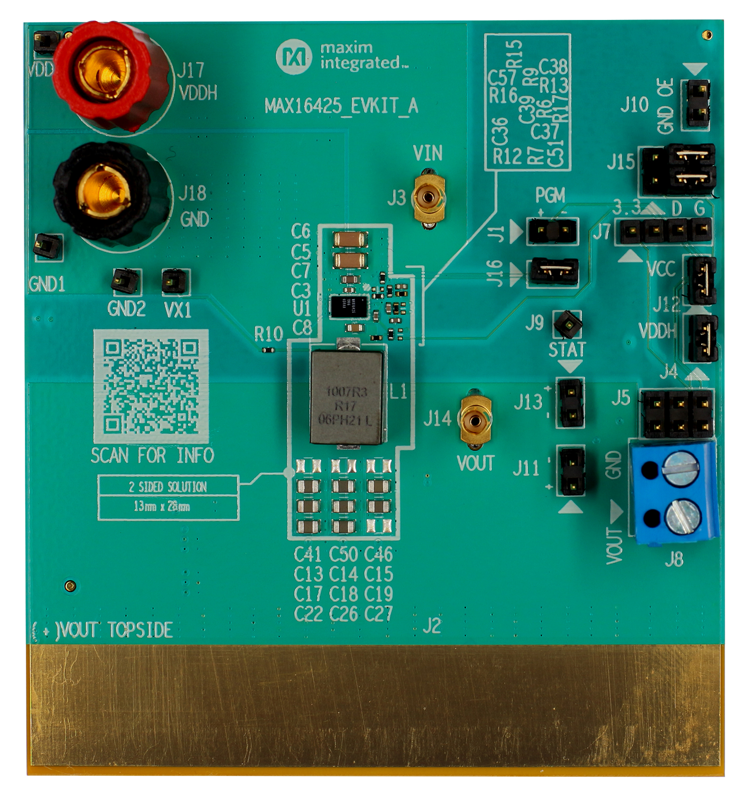
MAX16425/MAX16425A 评估套件
资料
最新评论
需要发起讨论吗? 没有关于 MAX16425的相关讨论?是否需要发起讨论?
在EngineerZone®上发起讨论