ADRV9032R
推荐用于新设计Integrated 2T2R TDD and FDD RadioVerse Transceiver with Dual Observation Paths
- 产品模型
- 2
概述
- 2 differential transmitters
- 2 differential receivers
- 2 differential observation receivers
- LO tunable range: 450 MHz to 7125 MHz
- RF range: 350 MHz to 7225 MHz1
- Maximum transmitter large-signal bandwidth: 200 MHz
- Maximum transmitter synthesis bandwidth: 450 MHz
- Maximum receiver signal bandwidth: 200 MHz
- Maximum observation receiver signal bandwidth: 450 MHz
- Fully integrated fractional-N RF synthesizer
- Fully integrated clock synthesizer
- Dual external LO inputs supporting operation up to 6 GHz
- JESD204B and JESD204C digital interface: up to 16.5 Gbps
- TDD and FDD operation
- Simplifying thermal and power consumption challenges
- 4.82 W power consumption for the TDD mode, enabled use case with 200 MHz iBW/OBW2
The ADRV9032R is a highly integrated, RF agile transceiver offering two transmitters, two observation receivers for monitoring transmitter channels, two receivers, integrated local oscillator (LO) and clock synthesizers, and digital-signal processing functions to provide a complete transceiver solution. The device provides the high radio performance and low-power consumption demanded by cellular infrastructure applications, software-defined radios, portable instruments, and military communications.
The receiver and transmitter signal paths use a zero-IF (ZIF) architecture that provides wide bandwidth with dynamic range suitable for non-contiguous multicarrier applications. The ZIF architecture has the benefits of low power and RF and bandwidth agility. The lack of aliases and out-of-band images eliminates anti-aliasing and image filters, reducing system size and cost, and making band independent solutions possible.
Please see the Data Sheet for the full description.
APPLICATIONS
- Software defined radios
- Portable instrumentation
- Military communications
- General-purpose radios
- Wireless infrastructure
- TDD and FDD applications
参考资料
数据手册 1
用户手册 1
ADI 始终高度重视提供符合最高质量和可靠性水平的产品。我们通过将质量和可靠性检查纳入产品和工艺设计的各个范围以及制造过程来实现这一目标。出货产品的“零缺陷”始终是我们的目标。查看我们的质量和可靠性计划和认证以了解更多信息。
| 产品型号 | 引脚/封装图-中文版 | 文档 | CAD 符号,脚注和 3D模型 |
|---|---|---|---|
| ADRV9032BBPZ-2T1 | 506-ball BGA_ED (19 mm x 19 mm x 1.76 mm) | ||
| ADRV9032BBPZRL-2T1 | 506-ball BGA_ED (19 mm x 19 mm x 1.76 mm) |
软件资源
API Device Drivers 1
Device Application Programming Interface (API) C code drivers provided as reference code allows the user to quickly configure the product using high-level function calls. The library acts as an abstraction layer between the application and the hardware. The API is developed in C99 to ensure agnostic processor and operating system integration. Customers can port this application layer code to their embedded systems/ Baseband Processor by integrating their platform-specific code base to the API HAL layer. To request this software package, go to the Software Request Form signed in with your MyAnalog account and under “Target Technology option - select “Wireless Communications" and choose processor/SOC as "ADRV9032R " , select the check box as well and submit the form. You will receive an email notification with a link for software download.
Evaluation Software 0
找不到您所需的软件或驱动?
硬件生态系统
| 部分模型 | 产品周期 | 描述 |
|---|---|---|
| 开关稳压器和控制器 1 | ||
| LT8625S | 推荐用于新设计 | 具有超低噪声的18V/8A降压型Silent Switcher 3 |
评估套件


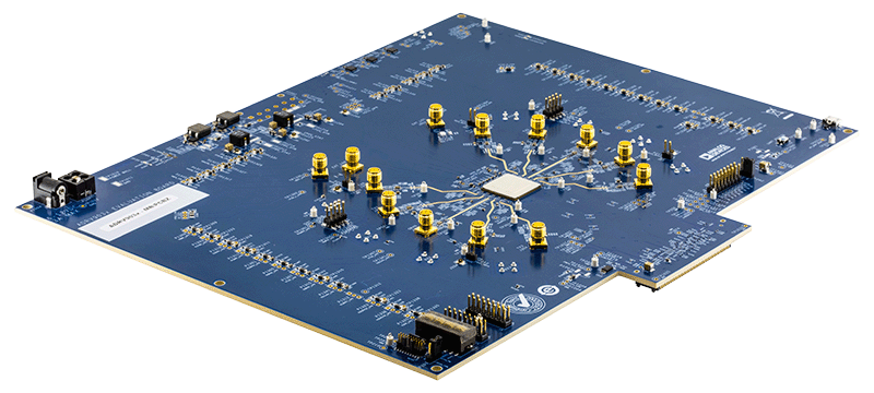
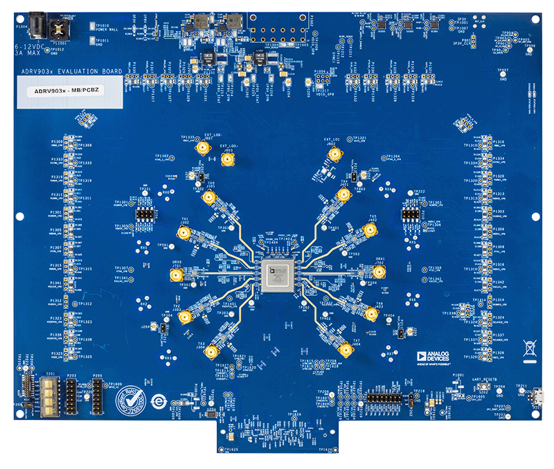
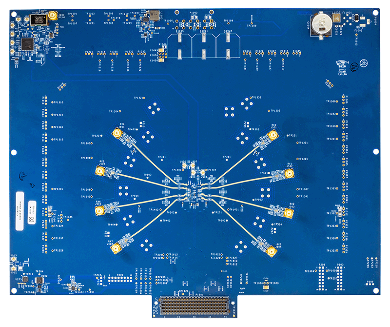
ADS10-V1EBZ Evaluation Board
资料
ADRV903x 评估系统用户指南
资料
软件
最新评论
需要发起讨论吗? 没有关于 ADRV9032R的相关讨论?是否需要发起讨论?
在EngineerZone®上发起讨论