AD4080
RECOMMENDED FOR NEW DESIGNS20-Bit, 40 MSPS, Differential SAR ADC
Low Noise, Low Power, Fast Precision SAR ADC
- Part Models
- 3
- 1ku List Price
- Starting From $55.99
Overview
- High performance
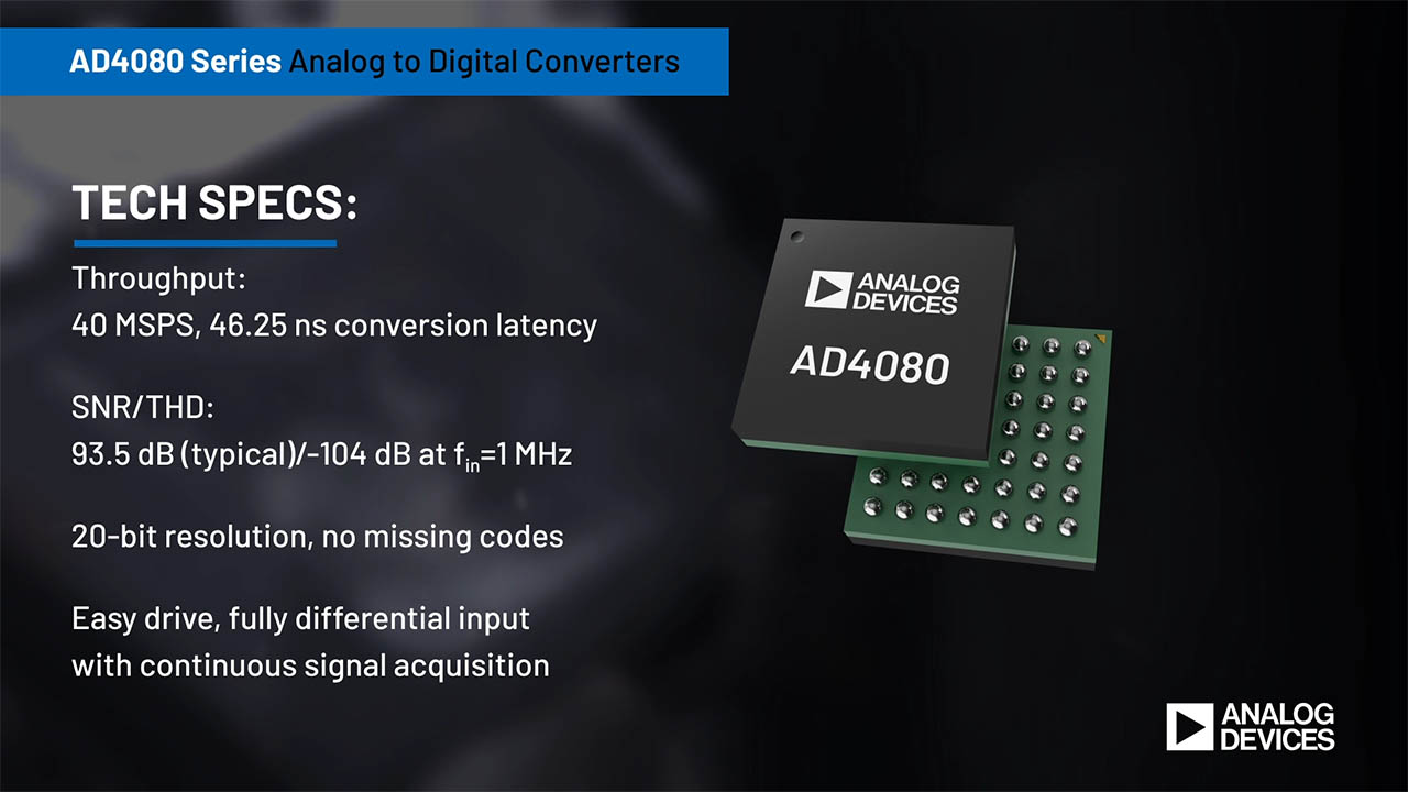
- Throughput: 40 MSPS, 46.25 ns conversion latency
- INL: ±4 ppm (typical), ±8 ppm (maximum)
- SNR/THD
- 93.6 dB (typical)/−110 dB (typical) at fIN = 1 kHz
- 93.5 dB (typical)/−104 dB (typical) at fIN = 1 MHz
- Noise spectral density: −167.6 dBFS/Hz
- 20-bit resolution, no missing codes
- Low power
- 79.3 mW typical at 40 MSPS with −0.5 dBFS sine-wave input
- Easy Drive, fully differential Input
- 6 V p-p differential input range
- Continuous signal acquisition
- Linearized, 5 μA/MSPS input current
- Integrated, low-drift reference buffer and decoupling
- Integrated VCM generation
- Digital features and data interface
- Conversion result FIFO, 16K sample depth
- Digital averaging filter with up to 210 decimation
- SPI configuration
- Configurable data interface
- Single lane, DDR, serial LVDS, 800 MBPS per lane
- Dual lane, DDR, serial LVDS, 400 MBPS per lane
- Single/quad lane SPI data interface
- Package
- 49-ball, 5 mm x 5 mm CSP_BGA, 0.65 mm pitch
- Integrated supply decoupling capacitors
- Operating temperature range: −40°C to +85°C
The AD4080 is a high-speed, low noise, low distortion, 20-bit, Easy Drive, successive approximation register (SAR) analog-to-digital converter (ADC). Maintaining high performance (signal-to-noise and distortion (SINAD) ratio > 90 dBFS) at signal frequencies in excess of 1 MHz enables the AD4080 to service a wide variety of precision, wide bandwidth data acquisition applications. Simplification of the input anti-alias filter design can be accomplished by applying oversampling along with the integrated digital filtering and decimation to reduce noise and lower the output data rate for applications that do not require the lowest latency of the AD4080.
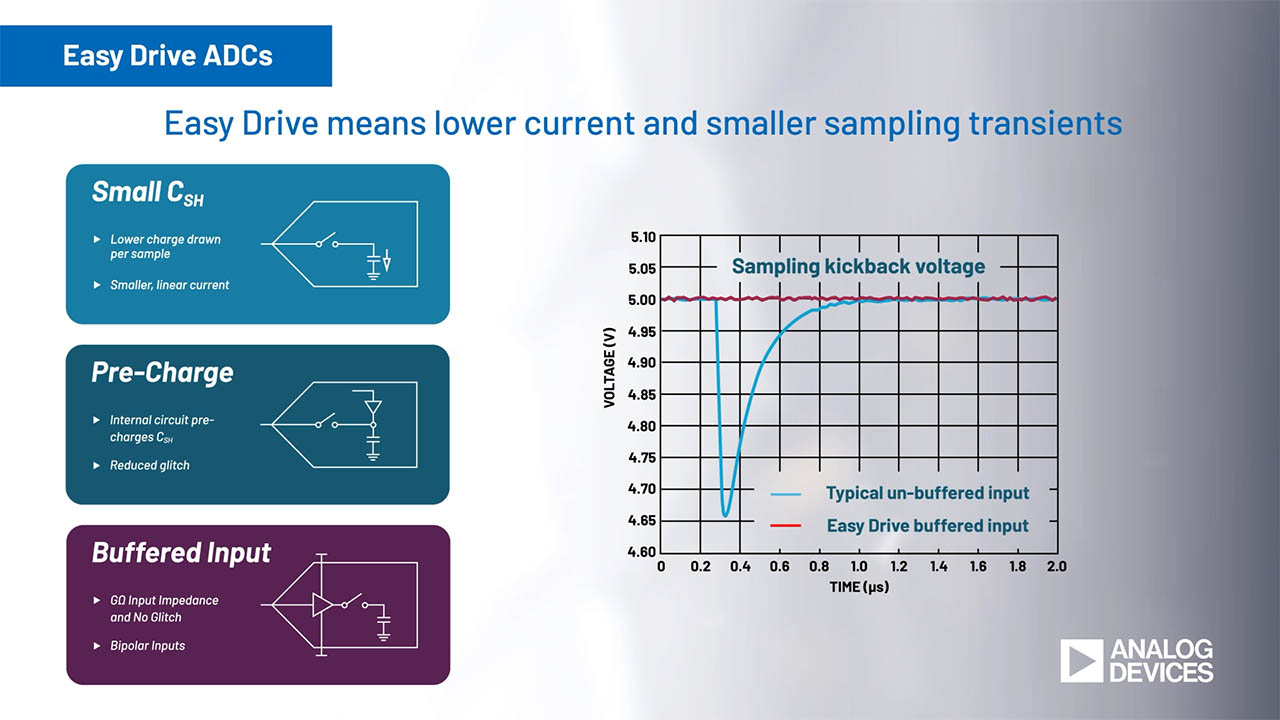
The AD4080 Easy Drive features reduce both signal chain complexity and power consumption while enabling greater channel density and flexibility in companion component selection. The product input structure was designed to minimize any input dependent signal currents; therefore, reducing any converter induced settling artifacts. The continuous acquisition architecture allows settling across the entire conversion cycle, easing ADC driver settling and bandwidth requirements as compared to other high-speed data converters.
The AD4080 includes several elements that simplify data converter integration: a low drift reference buffer, low dropout (LDO) regulators to generate ADC core and digital interface supply rails, and a 16K result data first-in first out (FIFO) that can greatly reduce the load on the digital host. Additionally, critical supply and reference decoupling capacitors are integrated in the package to ensure optimum performance, simplify printed circuit board (PCB) layout, and reduce the overall solution footprint.
APPLICATIONS
- Digital imaging
- Cell analysis
- Spectroscopy
- Automated test equipment
- High speed data acquisition
- Digital control loops, hardware in the loop
- Power quality analysis
- Source measurement units
- Electron and x-ray microscopy
- Radar level measurement
- Nondestructive test
- Predictive maintenance and structural health
Documentation
Data Sheet 1
User Guide 2
Video 2
Device Drivers 1
Webcast 2
ADI has always placed the highest emphasis on delivering products that meet the maximum levels of quality and reliability. We achieve this by incorporating quality and reliability checks in every scope of product and process design, and in the manufacturing process as well. "Zero defects" for shipped products is always our goal. View our quality and reliability program and certifications for more information.
| Part Model | Pin/Package Drawing | Documentation | CAD Symbols, Footprints, and 3D Models |
|---|---|---|---|
| AD4080BBCZ | 49-ball CSP_BGA (5 mm x 5 mm x 1.33 mm) | ||
| AD4080BBCZ-RL | 49-ball CSP_BGA (5 mm x 5 mm x 1.33 mm) | ||
| AD4080BBCZ-RL7 | 49-ball CSP_BGA (5 mm x 5 mm x 1.33 mm) |
| Part Models | Product Lifecycle | PCN |
|---|---|---|
|
Aug 19, 2025 - 25_0126 AD4080 Data Sheet Revision |
||
| AD4080BBCZ | PRODUCTION | |
| AD4080BBCZ-RL | PRODUCTION | |
| AD4080BBCZ-RL7 | PRODUCTION | |
This is the most up-to-date revision of the Data Sheet.
Software Resources
Device Drivers 1
Evaluation Software 4
Can't find the software or driver you need?
Hardware Ecosystem
-
Flow Cytometry Signal Chain -
Power Optimized Data Acquisition -
Low Noise Wideband Data Acquisition
| Parts | Product Life Cycle | Description |
|---|---|---|
| Differential Amplifiers 2 | ||
| ADA4945-1 | RECOMMENDED FOR NEW DESIGNS | High Speed, ±0.1 µV/˚C Offset Drift, Fully Differential ADC Driver |
| ADA4930-1 | RECOMMENDED FOR NEW DESIGNS |
Ultralow Noise Drivers for Low Voltage ADCs |
| Fanout Buffers 1 | ||
| AD9508 | RECOMMENDED FOR NEW DESIGNS | 1.65 GHz Clock Fanout Buffer with Output Dividers and Delay Adjust |
| LDO Linear Regulators 4 | ||
| LT3045 | RECOMMENDED FOR NEW DESIGNS | 20V, 500mA, Ultralow Noise, Ultrahigh PSRR Linear Regulator |
| ADP150 | PRODUCTION | Ultralow Noise, 150 mA CMOS Linear Regulator |
| MAX38912 | RECOMMENDED FOR NEW DESIGNS | 11µVRMS Low-Noise, 500mA LDO Linear Regulators with Low-Power Mode |
| LT3045-1 | RECOMMENDED FOR NEW DESIGNS | 20V, 500mA, Ultralow Noise, Ultrahigh PSRR Linear Regulator with VIOC Control |
| Operational Amplifiers (Op Amps) 1 | ||
| ADA4899-1 | PRODUCTION | Unity-Gain Stable, Ultralow Distortion, 1 nV/√Hz Voltage Noise, High Speed Op Amp |
| Phase-Locked Loop (PLL) Synthesizers 1 | ||
| ADF4350 | PRODUCTION | Wideband Synthesizer with Integrated VCO |
| Switching Regulators & Controllers 1 | ||
| LT8604/LT8604C | High Efficiency 42V/120mA Synchronous Bucks | |
| Voltage References 2 | ||
| LTC6655 | PRODUCTION | 0.25ppm Noise, Low Drift Precision References |
| ADR4530 | PRODUCTION | Ultra-Low-Noise, High-Accuracy 3.0V Voltage Reference |
Tools & Simulations
LTspice 1
Models for the following parts are available in LTspice:
- AD4080
IBIS Model 1
Signal Chain Designer
Signal Chain Designer is a web-based tool designed to create and simulate complex precision signal chains. See your circuit’s performance before you commit to your PCB: transfer function, noise, power consumption, input range, and DC error. Quickly experiment with different parts and architectures. Signal chains can be exported to LTspice for further analysis.
Open ToolLTspice® is a powerful, fast and free simulation software, schematic capture and waveform viewer with enhancements and models for improving the simulation of analog circuits.

