
Vibration Sensing Solutions
Vibration sensing is a critical measurement modality and the key predictive variable used to monitor and detect potential issues within rotating equipment. Early in the life cycle, these vibrations tend to be exceedingly small, so precision measurement is critical for early detection.
Analog Devices offers a complete line of vibration sensing components and solutions that provide an exceptional combination of high accuracy and robustness for condition-based monitoring (CBM), predictive maintenance, and other vibration applications.
Value and Benefits
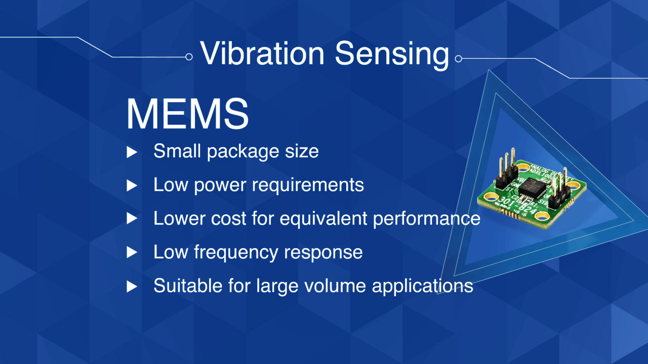
Capacitive-based MEMS accelerometers provide accurate detection while measuring vibration in performance-driven applications. MEMS capacitive accelerometers have taken a massive leap forward in performance, and our portfolio leads the industry in power, noise, bandwidth, and temperature specifications. MEMS capacitive accelerometers offer high levels of integration and functionality, with features such as self-test, peak acceleration, and spectral alarms. FFTs and data storage are shock-tolerant up to 10000g, have a DC response, and are smaller and lighter than piezoelectric accelerometers.


Enables high accuracy and robust vibration sensing for condition-based monitoring, predictive maintenance, and other vibration sensing applications
Provides reference designs to accelerate your vibration sensing design process
Offers platforms for developing both wired and wireless sensing solutions
Solution Resources
Piezoelectric Accelerometers
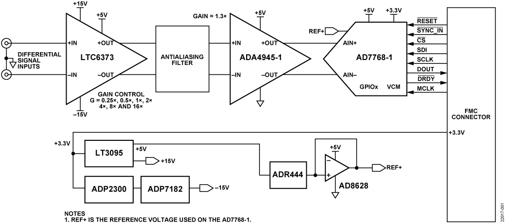
High Performance, Alias Free Measurement Platform for Flexible Data Acquisition System
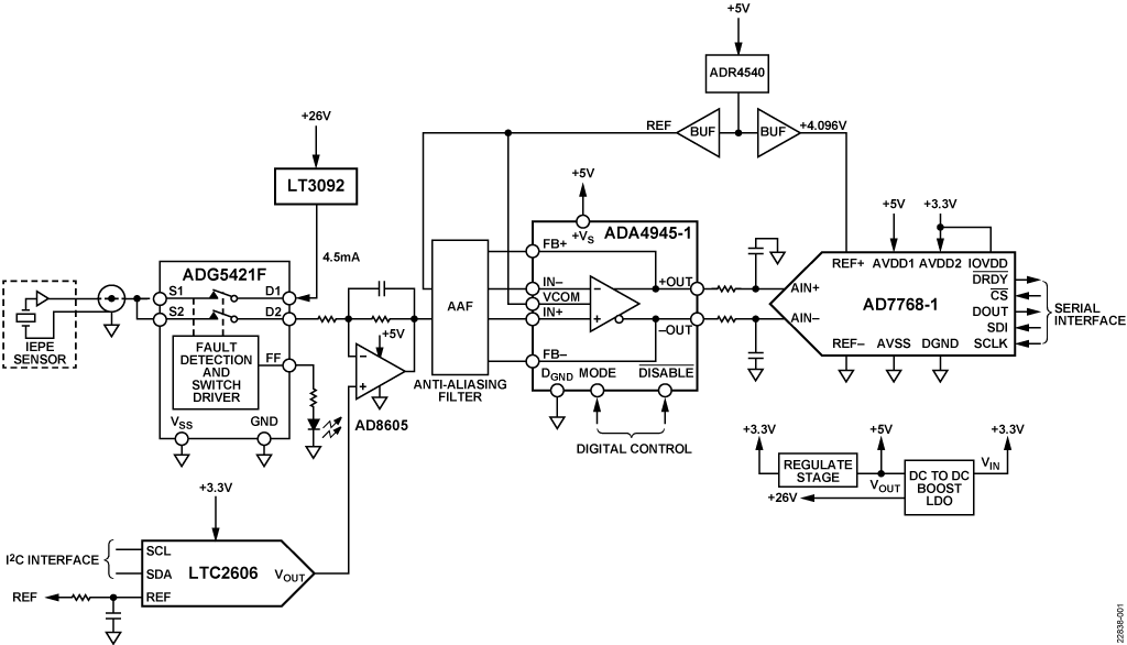

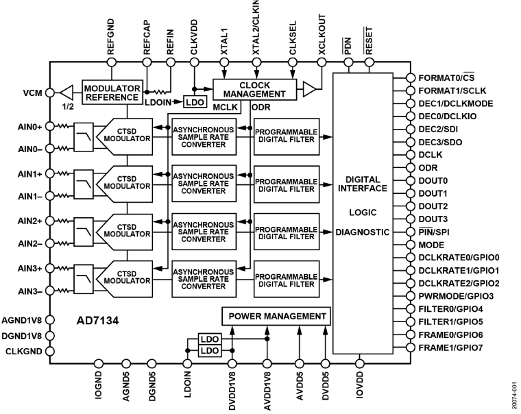
High Performance, Alias Free Measurement Platform for Flexible Data Acquisition System
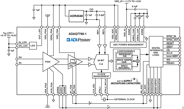
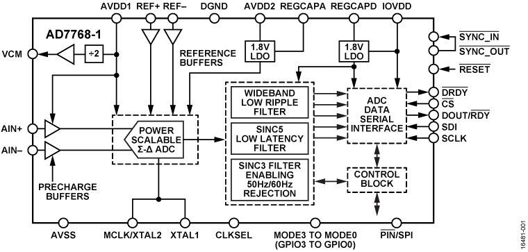
MEMS Capacitive Accelerometers

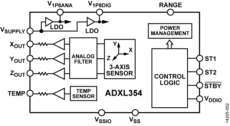
Low Noise, Wide Bandwidth, MEMS Accelerometer
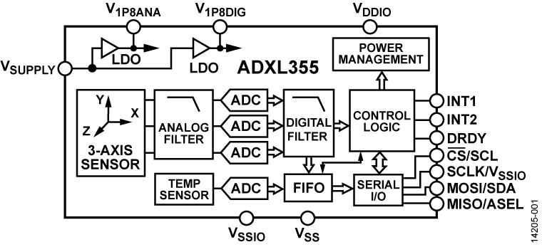
Low Noise, Low Drift, Low Power, 3-Axis MEMS Accelerometers with Digital Output
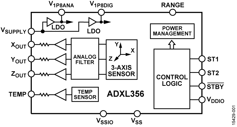
Low Noise, Wide Bandwidth, MEMS Accelerometer
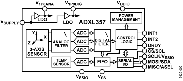
Low Noise, Low Drift, Low Power, 3-Axis MEMS Accelerometers with Digital Output
Interactive Signal Chains


Trainings and Tutorials

{{modalTitle}}
{{modalDescription}}
{{dropdownTitle}}
- {{defaultSelectedText}} {{#each projectNames}}
- {{name}} {{/each}} {{#if newProjectText}}
-
 {{newProjectText}}
{{/if}}
{{newProjectText}}
{{/if}}
{{newProjectTitle}}
{{projectNameErrorText}}