ADG5421F
RECOMMENDED FOR NEW DESIGNS±60 V Fault Protection and Detection, 11 Ω RON, Dual SPST Switch
- Part Models
- 1
- 1ku List Price
- Starting From $3.12
Overview
- Overvoltage fault protection up to ±60 V on S1 and S2 pins
- Power-off protection up to ±60 V on S1 and S2 pins
- Known state without digital inputs present
- Low on resistance of 11 Ω typical
- Ultraflat, on resistance
- Latch-up immune under any circumstance
- 3.5 kV human body model (HBM) ESD rating
- VSS to VDD −2 V signal range
- Fully specified at ±15 V, ±20 V, +12 V, and +36 V
- ±5 V to ±22 V dual-supply operation
- 8 V to 44 V single-supply operation
- 10-lead, 3 mm × 2 mm, LFCSP
The ADG5421F is a dual SPST, low on resistance switch that features overvoltage protection, power-off protection, and overvoltage detection on the source pins.
When no power supplies are present, the switch remains in the off condition, and the switch inputs are high impedance. When powered, if the analog input signal levels on either of the Sx pins exceed VDD or VSS by the threshold voltage, VT, both switches turn off together, and the open-drain fault flag (FF) pin pulls to a logic low. Input signal levels up to +60 V or −60 V relative to ground are blocked in both the powered and unpowered condition.
The switches turn on with a Logic 1 input and conduct equally well in both directions. The digital input is compatible with 1.8 V logic inputs over the full operating supply range.
APPLICATIONS
- Analog input and output modules
- Process control and distributed control systems
- Data acquisition
- Instrumentation
- Avionics
- Automatic test equipment
- Communication systems
- Relay replacement
Documentation
Data Sheet 1
User Guide 1
Design Note 1
Technical Articles 1
Video 4


Analog Dialogue 2
Webcast 1
ADI has always placed the highest emphasis on delivering products that meet the maximum levels of quality and reliability. We achieve this by incorporating quality and reliability checks in every scope of product and process design, and in the manufacturing process as well. "Zero defects" for shipped products is always our goal. View our quality and reliability program and certifications for more information.
| Part Model | Pin/Package Drawing | Documentation | CAD Symbols, Footprints, and 3D Models |
|---|---|---|---|
| ADG5421FBCPZ-RL7 | 10-Lead LFCSP (3mm x 2mm x 0.75mm) |
This is the most up-to-date revision of the Data Sheet.
Software Resources
Can't find the software or driver you need?
Request a Driver/SoftwareHardware Ecosystem
| Parts | Product Life Cycle | Description |
|---|---|---|
| Analog to Digital Converters (ADCs) 3 | ||
| AD7768-1 | RECOMMENDED FOR NEW DESIGNS | DC to 204 kHz, Dynamic Signal Analysis, Precision 24-Bit ADC with Power Scaling |
| AD4000 | PRODUCTION | 16-Bit, 2 MSPS/1 MSPS/500 kSPS, Precision, Pseudo Differential, SAR ADCs |
| AD4630-24 | RECOMMENDED FOR NEW DESIGNS | 24-Bit, 2 MSPS Dual Channel SAR ADC |
| Data Isolators 1 | ||
| MAX22665 | RECOMMENDED FOR NEW DESIGNS | Reinforced, Fast, Low-Power, Six-Channel Digital Isolators |
| Instrumentation Amplifiers 1 | ||
| LTC6373 | RECOMMENDED FOR NEW DESIGNS | 36V Fully-Differential Programmable-Gain Instrumentation Amplifier with 25pA Input Bias Current |
| LDO Linear Regulators 2 | ||
| ADP7182 | RECOMMENDED FOR NEW DESIGNS | –28 V, −200 mA, Low Noise, Linear Regulator |
| ADP7118 | RECOMMENDED FOR NEW DESIGNS | 20 V, 200 mA, Low Noise, CMOS LDO Linear Regulator |
| Low-Noise Amplifiers (LNAs) & Power Amplifiers 1 | ||
| MAX2244 | Obsolete | 2.5GHz, 22dBm/20dBm Power Amplifiers with Analog Closed-Loop Power Control |
| Operational Amplifiers (Op Amps) 1 | ||
| ADA4896-2 | RECOMMENDED FOR NEW DESIGNS | 1 nV/√Hz, Low Power, Rail-to-Rail Output Amplifiers |
| Switching Regulators & Controllers 1 | ||
| ADP5070 | PRODUCTION | 1 A/0.6 A, DC-to-DC Switching Regulator with Independent Positive and Negative Outputs |
| Voltage References 1 | ||
| LTC6655 | PRODUCTION | 0.25ppm Noise, Low Drift Precision References |
Tools & Simulations
LTspice 3
- Density Optimized LTspice Signal Chain Simulation
- LTC6373/LTC6655/ADG5421F Demo Circuit - Low Latency Programmable Gain Measurement for AD4630-24
- ADA4077/AD8675/LTC6655/ADG1236 Demo Circuit – Performance Optimized Sinewave Generation for AD5791
Models for the following parts are available in LTspice:
- ADG5421
- ADG5421F
IBIS Model 1
SPICE Model 1
LTspice® is a powerful, fast and free simulation software, schematic capture and waveform viewer with enhancements and models for improving the simulation of analog circuits.
Evaluation Kits

Evaluating the ADG5421F Fault Protection and Detection, 12 Ω RON, SPST Switch
Resources
Reference Designs


Quad-Channel IEPE Vibration Sensor Measurement System
Part Used
Design & Integration Tools


Precision Low Latency Development Kit
Part Used
Resources
Design & Integration Tools
Videos
-
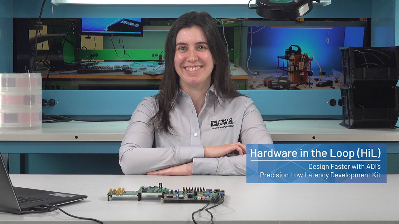 Low Latency Test and Measurement Kit – Hardware in the Loop
-
 Personalized Low Latency Hardware in the Loop (HiL) Solution


24-Bit Data Acquisition System for IEPE Sensors
Part Used
Resources
Design & Integration Tools
Videos
-
 Easily Connect Sensors with ADI's Robust Industrial Signal Chains
-
 CN0549 - CbM Development Platform