Overview
Design Resources
Design & Integration File
- Schematic
- Bill of Materials
- Gerber Files
- Allegro Layout Files
- Assembly Files
- Software Links
Evaluation Hardware
Part Numbers with "Z" indicate RoHS Compliance. Boards checked are needed to evaluate this circuit.
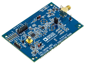
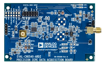
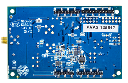
- EVAL-CN0540-ARDZ ($203.03) IEPE Compatible, DC Coupled, Single Channel CbM Data Acquisition Measurement System
Device Drivers
Software such as C code and/or FPGA code, used to communicate with component's digital interface.
FPGA/HDL
Features & Benefits
- IEPE compatible data acquisition system
- Piezo and MEMs sensors
- 54 kHz analog input bandwidth
- Arduino form factor compatible
Markets and Technologies
Parts Used
Documentation & Resources
-
CN0540 User Guide9/14/2020WIKI
-
Solutions For Rapid Prototyping: Answering the Needs of Practicing Engineers8/23/2023PDF784 K
-
CN0540: 24-Bit Data Acquisition System for IEPE Sensors (Rev. A)9/14/2020PDF899 K
Circuit Function & Benefits
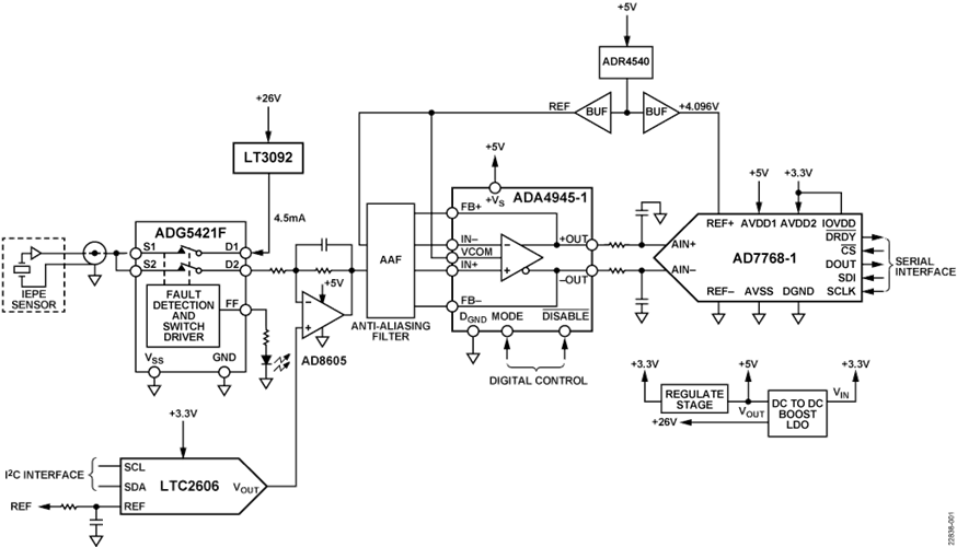
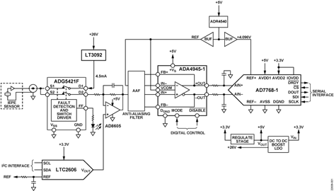
The reference design shown in Figure 1 shows a high resolution, wide bandwidth, high dynamic range, Integrated Electronics Piezoelectric (IEPE)-compatible interface data acquisition (DAQ) system that interfaces with IC Piezoelectric (ICP®)/IEPE sensors. The most common IEPE sensors are usually found in applications measuring vibration, but there are many IEPE sensors that measure parameters such as temperature, strain, shock, and displacement.
The focus of this circuit note is on the application of this solution to vibration applications, especially in the area of condition-based monitoring, but there is a large set of applications in instrumentation and industrial automation that use IEPE sensors in a similar way and that are served by similar signal chains.
Condition-based monitoring, in particular, uses sensor information to help predict changes in the condition of a machine. There are many methods of tracking the condition of a machine, but vibration analysis is the most commonly used method. By tracking the vibration analysis data over time, a fault or failure can be predicted, along with the source of the fault.
Vibration sensing in an industrial environment adds additional challenges because of the need for robust and reliable sensing methods. Knowing the condition of a machine helps increase efficiency and productivity and creates a safer working environment.
Most solutions that interface with piezoelectric sensors in the market are ac-coupled, lacking dc and subhertz measurement capabilities. The CN-0540 reference design is a dc-coupled solution in which dc and subhertz precision are achieved.
By looking at the complete data set from an IEPE vibration sensor in the frequency domain (dc to 50 kHz), the type and source of a machine fault can be better predicted using the position, amplitude, and number of harmonics found in the fast Fourier transform (FFT) spectrum.
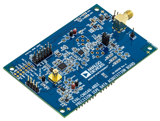
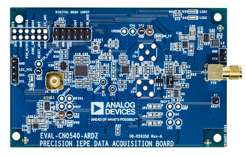
The data acquisition board is an Arduino-compatible form factor that can be interfaced and powered directly from most Arduino-compatible development boards.

Circuit Description
The circuit shown in Figure 1 is a data acquisition (DAQ) signal chain for an IEPE sensor consisting of a current source, level shifting and attenuation stage with a digital-to-analog converter (DAC), a third-order antialiasing filter, an analog-to-digital converter (ADC) driver, and a fully differential Σ-Δ ADC.
The programmable current source drives the piezoelectric accelerometer with constant current. The output current can be programmed by external resistors and is usually set between 2 mA and 20 mA, depending on the type of sensor and the cable.
The buffered and amplified output of the DAC, together with the level shifting op-amp, shifts the input signal close to a 2.5 V common-mode voltage (VOCM) to balance the input of the anti-aliasing filter and that of the fully differential amplifier (FDA). The second input of the FDA rail is set to 2.5 V, ensuring input headroom requirements are met, and the output is a fully differential voltage optimized for driving the ADC.
The antialiasing filter sets the bandwidth of the signal chain to 54 kHz. Piezoelectric accelerometers have bandwidths as high as 20 kHz, but a wider bandwidth signal chain has been chosen with respect to phase delay, achieving better phase matching performance in 3-axis measurements. (Further bandwidth limiting occurs in the digital filter of the ADCs, however, the phase delay is known and deterministic.)
ICP/IEPE VIBRATION SENSOR
Any IEPE vibration sensor can be interfaced with this CN-0540 reference design because all the IEPE vibration sensors work using the same principle with different offset voltages, noise levels, bandwidths, and sensitivities. An IEPE output signal carries both ac and dc voltages, where the vibration dependent ac voltage is dc shifted to some voltage level between 7 V and 13 V. This dc level varies from sensor to sensor, and for any given sensor, it has a drift component with respect to time, temperature, and excitation current.
The IEPE sensor must be powered by a current source with a sufficiently high voltage range to fully cover the amplitude of the sensor. A typical excitation voltage of the IEPE sensors is 24 V.
The input of the signal chain can receive a signal amplitude of up to 10 V p-p with an offset voltage up to 13 V. The dc offset is removed by applying a dc offset correction signal, allowing operation to an arbitrarily low frequency.

Figure 2 shows an ICP accelerometer block diagram of a sensor powered by a constant current source and connected to a dc-coupled signal chain. The maximum bandwidth of the sensor is proportional to the excitation current and inversely proportional to cable capacitance. The maximum desired output voltage of the sensor and cable type must be taken into account when choosing the level of the constant current, which can be determined by using the following equation:

where:
fMAX is the maximum frequency of the sensor in hertz.
IC is the constant current in mA.
1 mA is the power requirement of the sensor.
C is cable capacitance in pF.
V is the maximum peak voltage output from the sensor in volts.
Note that in Equation 1, 1 mA is subtracted from the total current supplied to the sensor (IC), where the approximate 1 mA is for powering the sensor itself and the rest of the current is for driving the cable. This number varies from sensor to sensor.
For example, this reference design was tested using an ICP accelerometer produced by PCB Piezotronics, Model 333B52 with a maximum peak output of 10 V, a 10 ft. cable length with a capacitance of 29 pF/ft., and an excitation current of 2.5 mA. Applying Equation 1, the maximum theoretical bandwidth of the sensor is 82.3 kHz. Neither the cable nor the chosen current level limit the performance of the sensor.
INPUT PROTECTION
Because IEPE sensors are typically connected to the DAQ system via long cables, and in an environment where many cables and other signal types are present, it is important to protect the DAQ system from any overvoltages that may occur due to operator miswiring or cable damage. The ADG5421F is an input protection switch that automatically detects overvoltage conditions and open circuits the sensor from the data acquisition signal path.
For the switches to be active, input signal levels from the sensor must be within the VSS − VT and VDD + VT range. Note that VSS is the negative power supply pin, VT is the voltage threshold, and VDD is the positive power supply pin.
The ADG5421F also provides a fault flag (FF) that can be used as an interrupt into a controller to alert the operator that an input fault has occurred. In normal operation, the FF pin is pulled high. However, if either the S1 pin or the S2 pin exceeds 26 V or 0 V by VT (0.7 V), the FF pin is pulled low to indicate a fault has occurred. If a fault is detected in the CN-0540, the sensor input and current source disconnects from the data acquisition system.
CONSTANT CURRENT SOURCE
Take care when designing the constant current source (CCS) and when considering noise performance. Low current noise is essential because current noise is converted to voltage noise when driving the input impedance of the signal chain.

Figure 3 depicts a 2-terminal current source with Resistors RSET and ROUT setting the output current to 4.5 mA and Capacitor CSET limiting the bandwidth of the current noise. The internal 10 μA reference current source of the LT3092 holds a stable VSET across RSET. The VSET is mirrored across ROUT, which sets the output current according to Equation 2.

Note that the actual IOUT current is 10 μA larger than the output current given by Equation 3 because of the internal reference current flowing from the SET terminal.
The data sheet recommends RSET = 20 kΩ to set the voltage drop across RSET to 200 mV, minimizing the effect of the offset voltage. (The offset voltage is more significant across a smaller VSET.) The white current noise produced by a resistor is given by Equation 3.

where:
T is absolute temperature in Kelvin.
k is Boltzmann’s constant in (J/K).
R is resistance.
Because resistor current noise is proportional to the square root of the inverse of resistance, increasing the value of RSET from the recommended 20 kΩ to 120 kΩ requires a proportional increase in ROUT as well (keeping the output current at the same level), causing a drop in the overall noise current. A capacitor, CSET, across RSET is recommended to lower the current noise of RSET and of the internal current reference of the LT3092. The CSET capacitor bypasses the current noise emitting from the LT3092.
An LT spice simulation of the constant current source, as shown in Figure 3, was performed to optimize component values and placement dependency. A nonideal voltage source was modeled, providing 0.7 mV rms voltage noise and 224 nA rms of current noise in a 20 MHz bandwidth, simulating a Keysight E3631 bench power supply with two outputs connected in series, set to 26 V total.
Table 1 lists rms noise for various combinations of component values. The rms current noise was simulated for a bandwidth from 1 mHz to 100 kHz. CCOMP acts like a high-pass filter, passing the noise from the voltage source to the output. Further increasing RSET and ROUT helps in the current noise reduction, but it also causes a higher voltage drop over the resistors, reducing the allowable signal swing.
| RMS Noise (nA) | RSET (kΩ) | ROUT (Ω) | CSET | CCOMP | |
| 158.8 | 20 | 80.6 | None1 | None1 | |
| 1273.5 | 20 | 80.6 | None1 | 100 nF | |
| 202.7 | 20 | 80.6 | None1 | 10 nF | |
| 15.5 | 20 | 80.6 | 100 nF | None1 | |
| 14.5 | 20 | 80.6 | 10 μF | None1 | |
| 3.1 | 120 | 470 | 10 μF | None1 | |
| 1 No Component Required. | |||||
When using a long cable with a high level of inductance, stability may become an issue. For more information on compensating inductive loads, refer to the LT3092 data sheet.
To calculate the usable sensor excitation voltage provided by the current source, use the following equation:

where:
VDD is the supply voltage of the constant current source.
LT3092DROP is the dropout voltage over the IC itself (typically 1.2 V at load current up to 10 mA).
RSET × 10 μA gives the dropout voltage over the resistor, which sets the output current level and a current from the internal 10 μA flows through the resistor.
In this case, the usable excitation voltage is 23.6 V.
VOLTAGE LEVEL SHIFTER
The voltage level shifter tolerates a sensor offset voltage up to 13 V, with a signal swing up to 10 V p-p, accommodating the majority of piezoelectric sensors on the market. An inverting voltage level shifter topology with an op-amp has been chosen, where a positive shifting voltage is required to bring the input voltage down to accommodate the FDA stage input requirements.

Figure 4 depicts an inverting voltage level shifter topology with an op-amp. Calculate the shifting voltage by the following equation:

The VOUT voltage produced by the voltage shifter is set to be as close to VOCM (2.5 V) as possible to balance the input of the FDA in the following stage. The RF/RIN ratio (the attenuation of the op-amp) must respect the following constraints:
- Supply voltage of the shifting op-amp: 5 V
- Range of the shifting voltage: 0 V to 5 V
- Stability of the op-amp
- Full-scale range of the ADC: ±4.096 V
- Input signal amplitude: 10 V p-p
- Input dc offset voltage: up to 13 V
An attenuation of 0.3 is a reasonable compromise, and a small gain in the following stage maximizes the input amplitude to the ADC and increases signal-to-noise ratio (SNR). Note that both the signal and noise at the output of the level shifter are amplified, so minimizing the output noise of the level shifter is critical.
A compromise has been made in CN0540 between input impedance and input noise, with an input noise level low enough and input resistance high enough to prevent introducing a measurement error. Piezoelectric sensors are generally low impedance output (hundreds of ohms) sensors and even a relatively low input impedance of the signal chain (tens of kΩ) introduces less than 1% of error. The final input impedance of RIN = 50 kΩ has been chosen as a compromise.
Use the following equations to calculate the voltage noise of the level shifter block with a shorted input:


where:
k is Boltzmann’s constant.
T is the absolute temperature in Kelvin.
R is the resistance in ohms.
All the contributions, excluding RIN, must be multiplied by the noise gain before squaring. The noise gain of an inverting op-amp configuration is the same as that of a noninverting configuration.

Use the following equation to calculate the inverting input op-amp noise contribution:

where NG is the noise gain of the circuit.
The single-pole RC filter at the voltage level shifter block limits the noise. Use the following equation, to calculate the rms value of noise produced by the voltage level shifter:

The noise contribution of the first stage is 20.8 μV rms, where the most significant noise contributor is the RIN, a consequence of setting the input impedance high enough to minimize errors due to loading.
DC BIAS COMPENSATING TECHNIQUE
Each IEPE accelerometer has a certain dc bias voltage that must be removed because this voltage does not carry any useful information. If dc coupling is used in a signal chain, the input voltage can be dc shifted to null the dc bias voltage, such that the ADC acknowledges only the ac portion of the input voltage without any dc offset. Precise dc shifting is crucial for accuracy in dc measurements and for maximizing the dynamic range of measurements.
An exact shifting voltage can be discovered using the shifting voltage in Equation 5. Following this approach, numbers of measurements at different temperatures must be taken for each board and sensor separately, thereby ensuing accuracy of the measurements.
Other, more precise, reliable, and automated techniques have been used. A custom successive approximation algorithm has been employed in the CN0540. Because the standard successive approximation model is estimating the final position of an unknown voltage level using a DAC to ADC control loop, this custom successive approximation is trying to set a mean voltage at the input of the ADC as close to 0 as possible using the DAC to ADC loop. In other words, the main goal is to set both inputs of the FDA to the same voltage level, which is VCOM = 2.5 V.
| Iteration | DAC Code | Next Move | Mean Voltage (mV) |
| 1 | 32,767 | Up | +4095.99 |
| 2 | 49,151 | Up | +1812.92 |
| 3 | 57,343 | Down | -339.57 |
| 4 | 53,247 | Up | +735.69 |
| ... | ... | ... | ... |
| 15 | 56,049 | Down | -0.366 |
| 16 | 56,048 | Final | -0.097 |
Table 2 shows the process of input bias voltage compensation using the successive approximation algorithm. Because a 16-bit DAC has been chosen, there are 16 iterations. At the very beginning of the process, the DAC is set to a half-scale output. Every time the DAC is set to a new value, the mean voltage is measured. If the mean voltage is positive, a 1-bit weight is added to the current DAC output. Otherwise, a 1-bit weight is subtracted from the current DAC output. The process is inverted due to the input op-amp being in an inverting configuration.

Equation 11 shows the bit weights being added or subtracted. 215 − 1 is the initial half-scale value followed by two ups and one down, meaning that the 14th and 13th bits are added and the 12th bit is subtracted.
The piezoelectric sensor itself produces a significant amount of voltage noise caused by the internal structure of the sensor. Upon the sensor being powered, environmental noise is picked up by the sensor all the time, resulting in even more noise converted from mechanical environmental events into voltage noise. To extract only the dc bias voltage of the piezoelectric sensor, and to remove quite a significant amount of noise (which is either random or periodical), a lot of averaging is taking place in the dc bias compensating process.
LEVEL SHIFTING DAC
A 16-bit voltage output DAC (LTC2606) with 27 selectable I2C addresses has been chosen for the level shifting. The DAC has a 2.5 V reference. To achieve the full 0 V to 5 V shifting voltage range preset at the noninverting input of the shifting op-amp, and to lower the DAC output voltage noise, an external buffer has been added. The buffer has the Sallen-Key structure with a cutoff frequency of 100 Hz and a gain of 2. The LSB of the DAC with a gained output follows:

There are also other gains on the path from the DAC to the ADC input. One LSB change observed by the ADC input is gained by 6.93 as a product of all the gains, giving an equivalent LSB size as follows:

where 2.667 is the gain of the FDA, and 1.3 is the gain of the shifting op-amp, which acts like a noninverting op-amp when a changing signal is brought to the noninverting input and the actual gain is 1 + (RF/RIN). The Equation 13 calculation gives the maximal theoretical dc error caused by shifting the sensor to the correct level.
Table 2 proves that one DAC LSB converted by the ADC is about 264 μV. Reviewing the last two ADC readings, the difference is only 1 LSB, resulting in 269 μV.

Figure 5 displays how the rms noise changes with only the input bias voltage applied to the input of the signal chain. Every time the input bias is changed, the DAC shifts the input to the correct level, ensuring a low offset error. The rms noise of the signal chain increases with the dc bias because the dc calibrator providing the dc bias produces more noise at higher voltage output levels.
As expected from Figure 5, the dynamic range responds to the increasing rms noise with the increasing input bias voltage in Figure 6.

Figure 7 displays the linearity of the system vs. the input bias voltage, using an input signal with a frequency of 1 kHz and an amplitude of 1 V p-p. Figure 7 shows that the input bias voltage has no significant impact on linearity and that the total harmonic distortion (THD) is stable.

Figure 8 displays the offset voltage error preset at the input of the ADC over temperature. The offset error was determined by running the input bias voltage compensation process over the temperature range with the same input voltage (10 V). The measurement at 25°C was set as 0 V of the offset error.

A voltage reference chip (ADR4540) with an output of 4.096 V was used, and the 2.5 V VOCM was derived from it.
DAC BUFFER
The internal buffer of the DAC limits the voltage noise and must be filtered. The DAC output must also be amplified to provide 0 V to 5 V because the DAC uses a 2.5 V reference.

Figure 9 depicts the level shifting DAC with a gained output using a low-pass Sallen-key filter structure. The cutoff frequency of the filter has been set to a low value of approximately 100 Hz using the following formula:

Because a gain is applied to the Sallen-key filter topology, the stability of the filter must be considered. Otherwise, the buffer is likely to become an oscillator. Another factor, related to the stability, is the quality (Q) of a filter that must be considered for this block. By keeping the Q factor low enough (at less than 0.707), it ensures that the frequency response has no peaking at the cutoff frequency and that the roll offs have gentler slopes and begin significantly sooner than at the cutoff frequency. A low Q factor is suitable for this application, where high linearity over frequency is desired. Note that the structure becomes unstable whenever the Q factor becomes negative. Use the following equation to determine the Q factor is determined:

where k is the gain of the Sallen-key topology, as follows:

For the values in Figure 9, the cutoff is 147.6 Hz, k is 2, and Q is 0.125, where stability and smooth roll off are ensured.
A comparison showing noise performance between the DAC shifting block with and without a buffer was made. Note that the signal chain used for this measurement has 12.3 μV rms of noise and 108.2 dB of dynamic range with shorted inputs. The rms noise was measured at a 64 kHz bandwidth.
Table 3 shows how output voltage changes with the DAC code. The DAC output was gradually set from zero to quarter scale, half scale, and up to three-quarter scale. In the worst case scenario, the DAC shifting block noise contribution is only 1.3 μV rms.
| DAC Code | Without Buffer | With Buffer | ||
| Noise | Dynamic Range | Noise | Dynamic Range | |
| 0x0000 | 12.71 μV rms | 107.3 dB | 13.1 μV rms | 107.5 dB |
| 0x3FFF | 24.52 μV rms | 101.9 dB | 13.4 μV rms | 107.2 dB |
| 0x7FFF | 25.21 μV rms | 101.1 dB | 13.6 μV rms | 107.5 dB |
| 0x9FFF | 26.39 μV rms | 101.2 dB | 13.6 μV rms | 107.3 dB |
ANTIALIASING FILTER AND FDA
The antialiasing filter and FDA use a differential multiple feedback low-pass structure with conversion from a single-ended to a differential signal. The cutoff frequency of the antialiasing filter has been set to 54 kHz, which is wider than the bandwidth of the majority of piezoelectric accelerometers. The filter provides a stopband rejection of −80 dB at 2.3 MHz.
The gain of this stage has been set to 2.667 to improve the SNR by boosting the input amplitude to more closely match the ±VREF range at the input of the ADC. The wideband noise is also amplified by the FDA, but this degradation is not as large as the improvement due to signal gain because the antialiasing filter limits wideband noise.
ANALOG-TO-DIGITAL CONVERSION
The AD7768-1, a precision, 1-channel, 24-bit, Σ-Δ ADC has been chosen for its excellent dc to 204 kHz bandwidth precision, low power consumption, typical 108.5 dB dynamic range, and −120 dB THD.
Use Equation 17 to calculate the output data rate of the ADC:

where:
MCLK is master clock.
MCLKDIV is a master clock divider factor.
FILTEROSR is the oversampling ratio (OSR) of a selected digital filter.
The clock divider and the filter OSR are register settings and can be changed over the SPI bus. OSRs for finite impulse response (FIR) and SINC5 filters are strictly set in the register map of the AD7768-1. A user can set the SINC3 filter to their own preferable OSR and change the output data rate by writing a specific value into a 12-bit SINC3 decimation rate register using the following equation:

where ODR is the desired output data rate in Hz, and 213 is the maximum possible value accepted by the SINC3 register. For example, the SINC3 register value for an output data rate of 4 Hz, with 16.384 MHz of MCLK, and a low power mode (MCLK/16) is 7999.
The default settings for this reference design are optimized for an ADC measurement bandwidth of 32 kHz, as follows:
- Power mode: low power mode
- MCLK divider: 16
- Filter type: FIR
- Filter decimation ratio: 32
- Input precharge buffers: enabled
- Reference buffers: precharge enabled
- VCM pin output: (AVDD1 − AVSS)/2
- Conversion length: 24 bits
- Conversion mode: continuous
- Checksum: no checksum
- Data read mode: continuous
- Status bit: disabled
- DRDY signal: enabled
Both buffers can be turned off when targeting a low power, demanding application. However, keeping the buffers on improves overall THD and SNR.
| ADC Power Mode | MCLK Ratio | Filter Type | Filter Decimation Rate | ODR (kSPS) | -3 dB Bandwidth (kHz) | RMS Noise (μV) |
| Fast | 2 | FIR | 32 | 256 | 110.8 | 10.98 |
| Medium | 4 | FIR | 32 | 128 | 55.4 | 10.94 |
| Medium | 8 | FIR | 64 | 64 | 27.7 | 7.37 |
| Low | 16 | FIR | 32 | 32 | 13.9 | 10.84 |
| Low | 16 | FIR | 1024 | 1 | 0.43 | 1.76 |
| Condition | MCLK/161 | MCLK/81 | |||
| Dynamic Range (dB) | Noise (μV rms) | Dynamic Range (dB) | Noise (μV rms) | ||
| DC-Coupled, CCS Enabled | |||||
| Shorted Input | 105.9 | 23.8 | 104.6 | 24.2 | |
| 1 kΩ at Input | 100.8 | 33.2 | 98.4 | 39.2 | |
| DC-Coupled, CCS Enabled | |||||
| Shorted Input | 105.7 | 21.3 | 105.4 | 22.1 | |
| 1 kΩ at Input | 105.9 | 22.2 | 105.2 | 22.1 | |
| 1 Low ripple FIR filter bandwidth = 0.433 x ODR. | |||||
MEASURED PERFORMANCE OF THE SIGNAL CHAIN
This signal chain design targets medium to wider bandwidth vibration sensing, where higher harmonics and frequency content above 1 kHz is important. In the design, here is a necessary trade-off between the system bandwidth, linearity, and the achievable noise performance. Higher input impedance is chosen to maintain signal accuracy (linearity), which in this design sets a maximum noise performance limit. The signal bandwidth is also set wider so that the response of the system over higher frequencies is maintained. A lower noise solution can be achieved with a design that has a narrower bandwidth, thus removing more of the wideband noise.
The CN-0540 sets the analog input bandwidth to 54 kHz, but the actual signal bandwidth is determined by the ADC configuration settings.
Noise
Noise performance of the entire signal chain was measured in several different scenarios.
Table 5 details the typical noise performance of the signal chain, without any sensor connected, as well as when a 1 kΩ load resistor is added. The results with the 1 kΩ resistor connected at the input of the signal chain indicates that the constant current source impacts the noise performance. The current noise is transformed to voltage noise and multiplied by the resistance of the 1 kΩ resistor, causing an elevation of the system noise.
Figure 10 shows the typical FFT plot for the system with shorted inputs. Figure 11 shows the dynamic range of the dc-coupled solution with shorted input over temperature.


Sensor Noise Contributions
The usual aim of the designer of a data acquisition system is to capture the sensor output signal as accurately as possible. What this means in practice is that the performance of the system should be set by the sensor characteristics. The noise performance of the sensor is often one of the key limiting factors to the overall measurement system, understanding this helps to set the performance requirement of the design.
For this design, the target was to support sensors that provide vibration data at bandwidths greater than 1 kHz, which are used in data acquisition systems targeted at condition-based monitoring for predictive maintenance on rotating or reciprocating plant equipment.
Table 6 details the performance level and bandwidth of a small selection of vibration sensors. The main considerations in sensor selection tend to be bandwidth, range, noise spectral density (NSD), and power.
The ADXL1002 and ADXL1004 sensors are low power devices suitable for a range of vibration applications, where power and bandwidth are important. These accelerometers are suitable for continuous monitoring applications, such as Internet of Things (IoT) machine monitoring.
| Sensor | Range (±g) | Output Range Peak-to-Peak (V) | Linearity (±%FSR) | NSD (μg/√Hz) | Flat Bandwidth (kHz) | Noise at Flat Bandwidth (μg rms) |
Dynamic Range at Flat Bandwidth (dB) |
| ADXL1002 | 50 | 4 | 0.1 | 25 | 11 | 2622 | 82.60 |
| ADXL1004 | 500 | 4 | 0.25 | 125 | 24 | 19365 | 85.23 |
| PCB 621B40 | 500 | 10 | 1 | 10 | 30 | 1732 | 104.95 |
| PCB 352C04 | 500 | 10 | 1 | 4 | 10 | 400 | 118.93 |
| PCB 333B52 | 5 | 10 | 1 | 0.4 | 3 | 22 | 98.50 |
For the highest sensitivities and bandwidths, where low noise and sensitivity at higher frequencies is key, piezoelectric sensors are still the most appropriate sensors to use. Because of the wide bandwidth and low noise capabilities of the AD7768-1, this signal chain is adapted to match the performance level of typical sensors in that wider bandwidth range beyond 10 kHz.
In the case of CN-0540, the system bandwidth is set to 54 kHz, and the signal chain noise performance is aimed at sensors that can achieve >100 dB dynamic range over that bandwidth. For example, Piezotronics PCB Model 621B40 accelerometer, which achieves almost 105 dB at 30 kHz.
This circuit can be adapted for sensors with higher dynamic range and narrower bandwidths by scaling the resistor values and gains of the stages and by utilizing the higher oversampling modes of the AD7768-1. A complete analysis is beyond the scope of this document, but more information on the trade-off between dynamic range and bandwidth using oversampling can be found in the AD7768-1 data sheet.
Linearity
The linearity of a sensor measurement system is important to give confidence that the measurement results do not vary due to variations in the output of the sensor. The measurement system accuracy should not vary as the output bias voltage or the signal amplitude of the sensor vary. Ideally, this accuracy should also be maintained as the temperature of the measurement system changes.
The CN-0540 was designed to be as linear as possible and to maintain that linearity over temperature so that less calibration of the measurement signal chain is required. The nonlinearity of the system to dc input voltage changes is reported as INL error. The nonlinearity of the system to sinewave inputs is reported as THD error.
The data in Figure 12 and Figure 13 show that the dc linearity (INL) is within ±10 ppm across a wide input voltage range and that both the INL and the THD are also relatively flat over a wide temperature range.


AC- vs. DC-COUPLED SOLUTION
The CN-0540 is aimed at dc-coupled application scenarios, where the dc component of the signal must be preserved or where the response of the system must be maintained down to frequencies below 1 Hz and lower. For this reason, the system is designed to handle the large dc bias of the IEPE sensor.
However, some systems may not require the response down to dc, and in those scenarios, an ac-coupled input channel is acceptable.
The main difference between the two solutions is complexity of a signal chain and precision at dc and low frequencies. Whereas the ac-coupled solution requires less complexity, it lacks precision at low frequencies.
The user can adapt this design to an ac-coupled design by inserting a coupling capacitor in series with the input resistor. Refer to the schematic files in the design support package for more information.
Inserting a coupling capacitor has the effect of changing the input response to a high-pass response, where the pole frequency is typically chosen to be much less than 0 Hz. This filter not only blocks the dc bias current but also removes some of the 1/f noise. The dynamic range of the ac-coupled system appears higher than the dc-coupled version, but this is only due to the removal of the low frequency noise. The tradeoff for this comes at the cost of reduced sensitivity to low frequency vibration measurement data.
A higher noise is also expected in dc-coupled solutions due to the DAC output and lack of a high-pass filter at the input of the signal chain. Figure 14 shows the response of the CN-0540 when ac-coupled with a high-pass cutoff frequency at 1 Hz. The measurement was taken with the shorted input of the signal chain and enabled constant current source, with the ADC in a low power mode, MCLK/16, and FIR filter with a decimation of 32, as per the dc-coupled measurements.

If implementing an ac-coupled solution, the correct type of capacitor must be selected to achieve the best performance. Ceramic capacitors, in general, suffer from noise production due to the piezoelectric effect, and nonlinearity due to voltage coefficient (change of the relative permittivity with respect to applied voltage) and dielectric absorption. Tantalum capacitors offer reasonable performance, and a wide range of capacitance values are manufactured as high as hundreds of μF. The tantalum capacitor in an ac-coupled scenario can achieve THD performance at a similar level to a dc-coupled system, but only at frequencies higher than 10 Hz. For accurate representation of lower frequency vibration, the dc-coupled version is preferred.
SYSTEM POWER
The CN-0540 is provided with an optimal power solution that allows the complete signal chain to be powered from a single 3.3 V rail.
Power Solution
Figure 15 shows a simplified block schematic of the power section of the CN-0540. For compatibility with microcontroller and other development boards with Arduino style connections, the power solution for the board has been designed to run from a single 3.3 V supply, which is typically provided by Arduino-compatible boards.
To ensure stability of the system, the microcontroller board should be able to supply at least 250 mA to the vibration monitoring board through the 3.3 V supply. This is in addition to any supply current that the microcontroller board itself takes from this supply.
Although the CN-0540 evaluation board does not need 250 mA in steady state operation, during the initial power-up phase, there may be inrush currents up to 200 mA or higher for up to 30 ms. If the microcontroller board cannot sustain this current, it may lead to a reset occurring on the microcontroller board. Check the current output specification for the microcontroller board if unexpected resets occur.

The power solution comprises three voltage domains: the 3.3 V domain, the 5 V domain, and the 26 V domain. It also includes the 2.5 mA current source for the IEPE sensor.
Arduino-compatible boards provide the IOREF supply that the CN-0540 uses directly, therefore, no power solution is needed. IOREF provides the digital interface supply to the AD7768-1 (IOVDD) and powers the 16.384 MHz master clock source.
The CN-0540 is compatible with IOREF voltages down to 1.8 V, allowing the CN-0540 board to interface to microcontroller boards with lower logic levels.
The purpose of the provided power solution circuitry is to allow the CN-0540 board to run from a single low voltage supply, which is typically available on a microcontroller board, and to generate the other required voltage rails from that one supply. On the CN-0540, the raw 3.3 V input supply rail is used directly to provide the digital interface logic power to the AD7768-1 (AVDD2 supply), and also provides the power to the dc-to-dc stages, which boost the voltage to 5 V and 26 V.
The first dc-to-dc stage boosts the 3.3 V to 7 V and then regulates to 5 V by the combination of the LTC3459 and ADP7118 devices to provide the clean supply rails required by the AD7768-1, the LTC2606, and the ADR4540 reference, as well as the associated amplifier stages.
The second dc-to-dc stage boosts the 3.3 V to 28 V, and then regulates to 26 V by the combination of the LT3494 and LT3008 devices. This clean 26 V rail is required to supply the LT3092 current source that provides the IEPE sensor with 2.5 mA at up to 26 V.
Power Measurements
Power measurements were taken directly from the 3.3 V and IOREF supply rails. The power measurements, therefore, include the contributions from the power solution components themselves.
The current to the 26 V rail is constant due to the constant current source and does not vary with ADC settings.
The power consumption of the rest of the system was measured in the different operation modes of the ADC. A 1 kΩ load resistor was placed at the input of the signal chain, to allow a path for the current flow from the constant current source and to maintain a dc bias at the input of the AD8605.
Power Consumption
The most significant register settings on the ADC that affect the power consumption are
- Power mode
- MCLK divider
- MCLK frequency
- Filter type
- Decimation ratio of the filter
- VCM pin output divider
- Analog input precharge buffers
- Reference buffers
- General-purpose input/outputs (GPIOs)
System Default Configuration
A default configuration of the system for narrow bandwidth measurement was chosen as follows for the ADC settings:
- MCLK divider: MCLK/16
- Power mode: low power mode
- FIR filter with decimation over 32
- VCM pin output: (AVSS − AVDD)/2
- Reference (REF) buffers: precharge on
- Analog input (AIN) buffers: precharge on
- MCLK frequency of 16.384 MHz
- FDA enabled, in low power mode
- DAC buffer enabled
- DAC output set to half scale
The system default configuration was used for most of the measurements included in this reference design.
| ADC Power Mode | ADC Data Rate (kSPS) | 3.3 V Rail (mA) | IOREF (mA) | Total Current (mA) | |
| Fast1 | 256 | 74 | 9 | 83 | |
| Median2 | 128 | 58 | 4 | 62 | |
| Low2 | 32 | 50 | 1 | 51 | |
| 1 FDA in full power mode. | |||||
| 2 FDA in low power mode. | |||||
The analog input and reference input buffers on the AD7768-1 are set to precharge mode. The ADA4945-1 FDA is set to low power mode. In full power mode, the FDA can provide wider bandwidth and better linearity performance. However, because the bandwidth of interest in this design is less than 50 kHz, low power mode is sufficient. By enabling the AD7768-1 internal precharge buffers, better linearity and better noise performance are achieved without significantly increasing the system power. For more information about matching driver amplifiers and using the input buffering options on the AD7768 family, see the Application Note AN-1384.
Common Variations
For higher channel count systems, the multichannel AD7768 and AD7768-4 are suitable alternatives to the AD7768-1. The ADC noise and linearity are similar to that of the AD7768-1, but these devices have the advantage of providing up to eight simultaneous channels in a single chip, which may simplify the implementation of a multichannel IEPE DAQ design.
Other ADCs that can be considered for vibration and condition monitoring signal chains are the AD4000, AD4002, and AD7380.
The ADA4610-1 is suitable for use in the first stage signal conditioning and for level shifting but requires higher supply voltages for correct operation. The ADA4807-1 and ADA4940-1 are alternatives for the ADC input antialiasing filter and driver stage.
The ADAQ7980/ADAQ7988 are 16-bit ADC μModule® data acquisition systems that integrate the ADC and the ADC driver stage, as well as the most critical passive components into a system in package (SiP) design. These devices are recommended where size or simplicity of implementation is more critical.
These options allow the signal chain components to be selected based on performance (noise or linearity), solution size, and cost.
Circuit Evaluation & Test
The following section outlines testing procedures and the gathering of the results for the CN-0540 circuit design. For complete details on the hardware and software setup, see the CN-0540 User Guide.
Equipment Needed
The following equipment is needed:
- EVAL-CN0540-ARDZ reference design board
- Terasic DE10-Nano FPGA
- FPGA Linux image with CN-0540 reference software
- Monitor with High-Definition Multimedia Interface (HDMI®) port
- HDMI to HDMI cable
- Wireless keyboard and mouse with USB dongle
- USB on-the-go (OTG) cable (micro USB to USB)
- Precision ac source (for example, AP2700, Brüel & Kjær, or similar precision sine generator)
- Coaxial cable with Bayonet Neill–Concelman (BNC) and Subminiature Version A (SMA) terminations

Getting Started
The basic test setup requires the EVAL-CN0540-ARDZ board to be plugged into the supported FGPA carrier board. The carrier board is required to power the EVAL-CN0540-ARDZ board, run the embedded Linux image, capture the data, and display the data. Software is available on the Analog Devices, Inc., website that supports the Terasic DE10-Nano and similar Arduino-compatible FPGA carrier boards.

To test the basic functionality of the board, connect a precision, high quality sine wave or arbitrary waveform generator to the analog input connector of the EVAL-CN0540-ARDZ board.
Step by step instructions follow:
- Mount the EVAL-CN0540-ARDZ evaluation board on the carrier board (Terasic DE10-Nano) by plugging into the Arduino headers as shown in Figure 18.

Figure 18. EVAL-CN0540-ARDZ Mounted on Terasic DE10-Nano Carrier Board - Connect the BNC end of the coaxial cable to the signal source single-ended or unbalanced output, and the other end to the EVAL-CN0540-ARDZ analog input SMA connector (see Figure 19).

Figure 19. Close Up Showing the Coaxial Cable Connected to the CN-0540 Analog Input Connector - Load the Analog Devices FPGA Linux image onto a micro SD card.
- Configure the micro SD card to use the correct files for both the CN-0540 and the carrier board.
- Connect the HDMI cable from the Terasic DE10-Nano to a monitor.
- Connect the USB OTG cable to the micro USB port on the Terasic DE10-Nano and insert the USB dongle for the wireless mouse/keyboard.
- Using the power supply provided, connect the barrel jack to the DE10-Nano, and turn on the Terasic DE10-Nano power switch.
- Power-on the sine or arbitrary waveform generator as follows:
- Set the signal type to sine wave.
- Set level to 1 V p-p at 1 kHz.
- Enable the output.
- Run the software and capture the resulting ADC data and FFT data.
The two plots in Figure 20 and Figure 21 show the typical captures that are expected from the carrier card when configured, as described in Step 1 through Step 9. Figure 20 shows the time domain view of the ADC capture data, illustrating the expected amplitude over a number of samples.

Figure 21 shows the same data processed and displayed as a frequency domain FFT plot.

For more information on the hardware and software setup, see the CN-0540 User Guide for complete details.
Piezoelectric Accelerometer Sensor Results
To achieve reasonable noise measurements, the piezoelectric accelerometer must be either stabilized using an active shaker table to cancel environmental vibrations or anchored to a massive object to reduce pickup of vibration from the environment. Where the piezoelectric accelerometer was connected directly to the input of the signal chain, anchoring to a massive object was used. The sensor used was a Piezotronics PCB Model 333B52, 3 kHz sensor.
Figure 22 shows a comparative performance plot of the FFT obtained while the sensor is connected. The noise of the system is dominated by the sensor signal.

I2C refers to a communications protocol originally developed by Philips Semiconductors (now NXP Semiconductors).”
