MAX16712
量产双路输出、6A、2MHz、2.7V至16V降压型开关稳压器
利用单个封装内的两个超快微型稳压器来缩小设计尺寸
- 产品模型
- 2
概述
- 功率密度高,元件数量少
- 双路输出或双相操作
- 单电源操作,并集成LDO用于偏置生成
- 紧凑型2.2mm x 3.5mm、28引脚WLP封装
- 内部补偿
- 宽工作范围
- 输入电压范围:2.7V至16V
- 输出电压范围:0.5V至5.8V
- 可配置开关频率:500kHz至2MHz
- 结温范围:–40°C至+125°C
- 三个编程引脚,用于选择不同的配置
- 每个输出都有独立的使能和电源良好指示
- 优化的性能和效率
- 峰值效率:90.5%(VDDH = 12V,VOUT = 1.8V,fSW = 1MHz)
- 交错式180°错相工作
- AMS可改善负载瞬态
- 可选DCM可提高轻负载效率
- 主动电流均衡支持双相操作
MAX16712是一款完全集成式双路输出高效降压型DC-DC开关稳压器。该器件采用2.7V至16V的输入电源工作,每路输出都可在0.5V至5.8V之间调节。该IC每路输出可提供高达6A的负载电流。两个输出可以并联成为一个单路输出、双相稳压器,从而支持高达12A的负载电流。
该器件的开关频率可在500kHz至2.0MHz之间进行配置,并能够优化解决方案的尺寸和性能设计。
MAX16712采用具有内部补偿的固定频率、电流模式控制。双路开关稳压器以180°错相运行。该IC采用先进的调制方案(AMS)和可选的断续电流模式(DCM)工作,以提高性能。另外也可以通过将引脚绑定电阻从PGM0引脚连接到地,来选择操作设置和可配置功能。
MAX16712具有内部1.8V LDO输出,为栅极驱动(VCC)和内部电路(AVDD)供电。
MAX16712集成了多种保护功能,包括正负过流保护、输出过压保护和过温保护,可确保设计稳定可靠。
该器件采用紧凑型2.2mm x 3.5mm晶圆级封装,支持的结温范围为-40℃至+125℃。
应用
- 通信设备
- FPGA/DSP/MCU的I/O引脚
- 存储器 VDDQ
- 网络设备
- 负载点(POL)稳压器
- 服务器和存储设备
- μP芯片组
参考资料
数据手册 1
视频 1

ADI 始终高度重视提供符合最高质量和可靠性水平的产品。我们通过将质量和可靠性检查纳入产品和工艺设计的各个范围以及制造过程来实现这一目标。出货产品的“零缺陷”始终是我们的目标。查看我们的质量和可靠性计划和认证以了解更多信息。
| 产品型号 | 引脚/封装图-中文版 | 文档 | CAD 符号,脚注和 3D模型 |
|---|---|---|---|
| MAX16712AWI+ | WLCSP | ||
| MAX16712AWI+T | WLCSP |
这是最新版本的数据手册
软件资源
找不到您所需的软件或驱动?
申请驱动/软件工具及仿真模型
EE-Sim Power®工具 1
EE-Sim DC-DC转换器工具可根据您的要求快速创建完整的电源设计,包括原理图、BOM(采用市售部件)、时域和频域仿真。您可以下载自定义原理图,在独立EE-Sim OASIS仿真器中进一步分析,其中采用SIMPLIS和SIMetrix SPICE引擎。
立即开始EE-SimSIMPLIS Models 1
评估套件
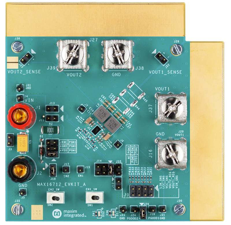
MAX16712评估套件
资料
最新评论
需要发起讨论吗? 没有关于 MAX16712的相关讨论?是否需要发起讨论?
在EngineerZone®上发起讨论