LT8646SA
推荐用于新设计65V、8A 同步降压静音开关电源 2,静态电流 2.5μA
- 产品模型
- 4
概述
- Silent Switcher® 2 架构
- 可在任何 PCB 上实现超低 EMI 发射
- 消除了 PCB 布局敏感性
- 内部旁路电容器可降低发射的 EMI
- 可选的扩频调制功能
- 在高频下具有高效率
- 在 400kHz、24VIN 至 5VOUT 范围内效率高达 94%
- 在 1MHz、24VIN 至 5VOUT 范围内效率高达 93%
- 宽输入电压范围:3.4V 至 65V
- 宽输出电压范围:0.97V 至 (VIN - 0.5V)
- 超低静态电流 Burst Mode 工作模式
- 2.5μA IQ,将 12VIN 调节为 3.3VOUT(LT8645SA)
- 输出纹波 < 10mVP-P
- 外部补偿:快速瞬态响应和电流共享(LT8646SA)
- 稳健的高 VOUT 运行
- 安全承受高反向电流
- 快速最短开关接通时间:40ns
- 在所有条件下均具有低压降:1A 时 60mV
- 可调并且可同步:200kHz 至 2.2MHz
- 输出软启动和追踪
- 小型 32 引脚 6mm × 4mm LQFN 封装
- 通过 AEC-Q100 汽车应用认证
LT8645SA/LT8646SA 同步降压稳压器采用第二代静音开关架构,旨在最大限度地减少 EMI 辐射,同时在高开关频率下提供高效率。®这包括集成旁路电容器,以优化内部所有快速电流回路,并通过消除布局敏感性,轻松实现所宣传的 EMI 性能。
快速、干净、低过冲的开关边沿即使在高开关频率下也能实现高效率运行,从而实现较小的整体解决方案尺寸。峰值电流模式控制,最小导通时间为 40ns,即使在高开关频率下也能实现高降压比。LT8646SA 具有外部补偿功能,可在高开关频率下实现电流共享和快速瞬态响应。
突发模式® 运行可实现超低待机电流消耗,强制连续模式可控制整个输出负载范围内的频率谐波,或者扩频运行可进一步降低 EMI 辐射。
应用
- 汽车和工业电源
- 通用降压型转换器
参考资料
数据手册 1
用户手册 1
ADI 始终高度重视提供符合最高质量和可靠性水平的产品。我们通过将质量和可靠性检查纳入产品和工艺设计的各个范围以及制造过程来实现这一目标。出货产品的“零缺陷”始终是我们的目标。查看我们的质量和可靠性计划和认证以了解更多信息。
| 产品型号 | 引脚/封装图-中文版 | 文档 | CAD 符号,脚注和 3D模型 |
|---|---|---|---|
| LT8646SAAV#PBF | 32-Lead LQFN (6mm x 4mm x 0.94mm w/ EP) | ||
| LT8646SAAV#TRPBF | 32-Lead LQFN (6mm x 4mm x 0.94mm w/ EP) | ||
| LT8646SAAV#WPBF | 32-Lead LQFN (6mm x 4mm x 0.94mm w/ EP) | ||
| LT8646SAAV#WTRPBF | 32-Lead LQFN (6mm x 4mm x 0.94mm w/ EP) |
软件资源
找不到您所需的软件或驱动?
申请驱动/软件工具及仿真模型
LTspice
LTspice中提供以下器件型号:
- LT8646S
- LT8646SA
LTpowerCAD
LTpowerCAD中提供以下器件的设计工具:
- LT8646S
LTspice®是一款强大高效的免费仿真软件、原理图采集和波形观测器,为改善模拟电路的仿真提供增强功能和模型。
评估套件
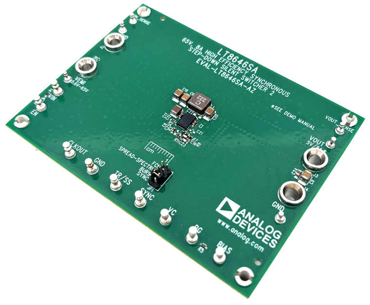
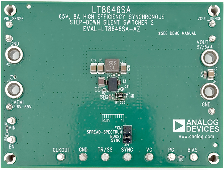
65V,8A 同步降压静音开关 2
资料
最新评论
需要发起讨论吗? 没有关于 LT8646SA的相关讨论?是否需要发起讨论?
在EngineerZone®上发起讨论