

Overview
Design Resources
Design & Integration File
• Schematic• Bill of Materials
• Assembly Drawing
• Allegro Layout Files
• Gerber Files Download Design Files 925.21 K
Evaluation Hardware
Part Numbers with "Z" indicate RoHS Compliance. Boards checked are needed to evaluate this circuit.
- EVAL-CFTL-LVDT ($112.34) Measurement Specialties LVDT Sensor
- EVAL-CN0371-SDPZ ($60.92) Low Power LVDT Signal Conditioner with Synchronous Demodulation
- EVAL-SDP-CB1Z ($134.00) Eval Control Board
Device Drivers
Software such as C code and/or FPGA code, used to communicate with component's digital interface.
AD719x GitHub no-OS Driver Source Code
AD7192 IIO High Precision ADC GitHub Linux Driver Source Code
Features & Benefits
- LVDT Signal Conditioner
- Low Power
- Synchronous Detection
Product Categories
Markets and Technologies
Parts Used
Documentation & Resources
-
UG-277: SDP-B Controller Board12/8/2010PDF605 kB
-
CN-0371: Low Power LVDT Signal Conditioner with Synchronous Demodulation3/23/2015PDF392 K
Circuit Function & Benefits
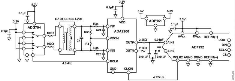
The circuit shown in Figure 1 is a complete linear variable differential transformer (LVDT) signal conditioning circuit that can accurately measure linear position or linear displacement from a mechanical reference. Synchronous demodulation in the analog domain is used to extract the position information and provides immunity to external noise. A 24-bit, Σ-Δ analog-to-digital converter (ADC) digitizes the position output for high accuracy.
LVDTs utilize electromagnetic coupling between the movable core and the coil assembly. This contactless (and hence frictionless) operation is a primary reason for why they are widely used in aerospace, process controls, robotics, nuclear, chemical plants, hydraulics, power turbines, and other applications where operating environments can be hostile and long life and high reliability are required.
The entire circuit, including the LVDT excitation signal, consumes only 10 mW of power. The circuit excitation frequency and output data rates are SPI programmable. The system has a programmable bandwidth vs. dynamic range trade-off. It supports bandwidths of over 1 kHz, and at a bandwidth of 20 Hz, the circuit has a dynamic range of 100 dB, making it ideal for precision industrial position and gauging applications.


Circuit Description
The ADA2200 synchronous demodulator extracts position information by filtering the LVDT secondary signal before demodulating the signal to a low frequency output voltage that is proportional to the LVDT core displacement. The ADA2200 drives the AD7192 24-bit Σ-Δ ADC, which digitizes and filters the output. The ADA2200 generates the synchronous LVDT excitation signal, and the ADG794 switch converts the CMOS level excitation signal into a precision 3.3 V square wave to drive LVDT primary winding.
The LVDT is an absolute displacement transducer that converts a linear displacement into a proportional electrical signal. An LVDT is a specially wound transformer with a moveable core that is affixed to the position to be measured. An excitation signal is applied to the primary windings. As the core moves, the voltage on the secondary windings changes proportionally, and from this voltage, position is calculated.
There are many types of LVDTs and different ways of extracting position from them. The Figure 1 circuit uses the LVDT in 4-wire mode. The two LVDT secondary outputs are connected such that the voltages oppose each other, performing a subtraction. When the LVDT core is in its null position, the voltages on each of the two secondaries are equal, and the voltage difference across the two windings is zero. As the core moves from the null position, the difference voltage across the secondary windings increases. The phase of the LVDT output voltage changes based on direction.
The master clock for this circuit is generated by the AD7192 ADC. The ADA2200 accepts the master clock and generates all of its internal clocks, including the reference clock used as the LVDT excitation signal. The clock dividers on the ADA2200 are configured to provide an excitation signal of 4.8 kHz. The ADG794 converts the excitation signal to a precision ±3.3 V square wave from the ADC supply voltage. The 3.3 V supply is also used as the ADC reference voltage; therefore, the ratiometric relationship between the excitation signal and ADC reference voltage improves the noise and stability performance of the circuit. The 3.3 V for the system is supplied by an ADP151 low dropout regulator driven from a 5 V supply.
The coupling circuit between the LVDT secondary windings and the ADA2200 input is used to band limit the signal and to adjust the relative phase between the RCLK and ADA2200 input. The circuit is configured to maximize the quadrature (Phase = 90°) response and to minimize the in-phase (Phase = 0°) response. This enables the position to be determined by only measuring the quadrature output and makes the ADA2200 output voltage less sensitive to phase variations in the circuit. The main sources of phase variation come from temperature changes in the LVDT that cause its effective series resistance and inductance to change.
The antialiasing filter at the ADA2200 output maintains the signal bandwidth supported by the ADC. The output bandwidth of the AD7192 internal digital filter is approximately 0.27 times the output data rate. To maintain the output bandwidth at the maximum output date rate of 4.8 kHz, the output antialiasing filter −3 dB corner frequency is set to approximately 2 kHz. For systems requiring lower output data rates, the antialiasing filter corner frequency can be reduced accordingly.
Integrated Synchronous Demodulator
The ADA2200 integrated synchronous demodulator forms the core of the circuit. It uses a unique charge sharing technology to perform discrete time signal processing in the analog domain. The signal path of the ADA2200 is completely differential. It consists of a high impedance input buffer followed by a fixed low-pass filter (FIR decimation filter), a programmable IIR filter, a demodulator, and a differential output buffer. It has an input and output common-mode voltage equal of 1.65 V (½ of the 3.3 V supply voltage).
The ADA2200 accepts the 4.92 MHz clock from the AD7192 ADC and generates all of its internal clocking signals as well as the 4.8 kHz reference clock used as the LVDT excitation signal. The ADA2200 has configurable clock dividers that can be programmed to support many different excitation frequencies.
CMOS Switch
The ADG794 CMOS switch was chosen for the low on resistance of the switches, fast switching times, break-before-make switching action, and low cost.
The ADG794 converts the low voltage CMOS-level RCLK output of the ADA2200 into a low impedance differential output square wave source, which drives the LVDT. To provide headroom for the switches to drive the positive 3.3 V signal, the ADG794 VDD input is supplied from the 5 V power supply.
LVDT
The Figure 1 circuit supports a wide variety of LVDTs with minor modifications. The E-100 LVDT from Measurement Specialties, Inc., was used in 4-wire mode to demonstrate the main attributes of the circuit. The E-100 has a stroke range of ±2.54 mm, an output sensitivity of 240 mV/V at the stroke ends, and a maximum linearity error of ±0.5% of full-scale range. The operating frequency range is from 100 Hz to 10 kHz. See the E-Series LVDT data sheet for complete details.
ADA2200 Input Coupling Network
The ADA2200 input coupling network can be tuned for different LVDTs. The inductance of the LVDT secondary windings and the shunt capacitor (C4) form a tank circuit. The R4 and R33 resistors reduce the Q of the tank circuit, making the circuit less sensitive to changes in the LVDT winding inductance and resistance at the expense of increased power consumption. The pair of RC filters created by R34/C24 and R35/C25 reduces the signal bandwidth and provides additional degrees of freedom for adjusting the relative phase of the circuit. The maximum output from the ADA2200 internal phase sensitive detector (PSD) occurs at relative phase shifts of 0° or 180°.
For the E-100 LVDT with a 4.8 kHz square wave excitation, the optimum phase for maximum output is achieved for the following component values:
- R4 = R33 = 2.2 kΩ
- R34 = R35 = 1 kΩ
- C24 = C25 = 3300 pF
- C4 = 0.01 μF
To tune the circuit, the phase can be measured by placing the LVDT core to produce a near full-scale output signal. Next, make in-phase (I) and quadrature (Q) output signal measurements. From these measurements, the relative phase is calculated as follows:

Adjusting the network components until the absolute value of θREL is less than approximately ±3° improves the circuit sensitivity to variation in the LVDT electrical parameters.
ADC Selection and Synchronization
The AD7192 Σ-Δ ADC was chosen because it supports a configurable output data rate and has different digital filter output options, thereby allowing trade-offs between bandwidth and noise. The master clock output feature makes it easy to lock the frequency of the ADC sample clock to the ADA2200 output signal. This is required to optimize the performance of the digital filters. The desired value for determining the position from the LVDT signal is the average value over one excitation clock period. Therefore, when the AD7192 output date rate is set to 4.8 kHz, exactly one excitation clock period, the desired average is obtained. If the excitation clock period and ADC sampling frequency are not locked, an error is induced in the recovered position measurements. Dividing the output data rate is effectively taking the average over multiple excitation clock periods.
The digital filter performance can be analyzed in the frequency domain as well. Even when the LVDT core position is fixed, the ADA2200 output signal contains energy at multiples of the excitation signal frequency. These frequency components are spurious error sources. The AD7192 has a sinc3 or sinc4 transfer function with transfer function zeros at multiples of the output data rate. The output spurs are rejected by setting the output data rate of the ADC to the excitation signal frequency (or submultiples of the excitation frequency). If the excitation clock period and ADC sampling frequency are not locked, the spurs will not fall in the nulls of the transfer function.
A complete set of documentation for the circuit including schematics, layouts, and bill of materials can be found at www.analog.com/CN0371-DesignSupport.
User Software for Performance Analysis
The circuit is supported with a graphical user interface that facilitates configuring the devices on the board and evaluating the circuit performance. Tabs are available for performing circuit calibration and device configuration, as well as for displaying noise performance, linearity performance, and real time position measurements. For a complete description of the software package, see the CN-0371 Software User Guide.


Noise Analysis
The output noise of the circuit is a function of the ADC output data rate. Table 1 shows the effective number of bits (ENOB) in the digitized data vs. the ADC sample rate, assuming a 2.5 V full-scale output voltage. The noise performance of the circuit is independent of the LVDT core position.
| ADS Data Rate (SPS) | Output Bandwidth (Hz) | ENOBs (RMS) | ENOBs (P-P) |
| 4800 | 1300 | 14.0 | 11.5 |
| 1200 | 325 | 14.9 | 12.4 |
| 300 | 80 | 15.8 | 13.3 |
| 75 | 20 | 16.2 | 13.6 |
If the ADA2200 output noise were frequency independent, the expected effective number of bits would increase by one bit for every four-fold decrease in the output data rate. The diminishing increase in ENOBs at the lower output data rates is caused by the 1/f noise of the output driver that begins to dominate the noise floor at the lower output data rates.
Linearity Test Results
The linearity results were measured by first performing a two-point calibration at core displacements of ±2.0 mm. From these two measurements, the slope and offset were determined to establish an expected straight line fit. Next, measurements were taken at core displacements across the full-scale range of ±2.5 mm. The measured data was subtracted from the expected straight line fit data to determine the linearity error.


The measured data shows that the circuit performance is better than the linearity specified in the E-Series LVDT data sheet.
Synchronous Operation of Multiple LVDTs
In many applications, multiple LVDTs are used in close proximity. If the LVDTs operate at similar carrier frequencies, stray magnetic coupling can cause generation of beat notes. The resulting beat notes can interfere with the accuracy of measurements made under these conditions. To avoid this situation, all LVDTs must be synchronized.
Multiple ADA2200 devices can be synchronized by bringing the devices out of reset simultaneously. The ADA2200 leaves reset mode on the first rising edge of CLKIN after the RST pin is deasserted. Therefore, driving all of the ADA2200 CLKIN pins from a single source and all of the RESETB lines from a single source is sufficient to ensure the devices operate synchronously. Avoid deasserting RESETB near the rising edge of CLKIN to prevent the device resets from occurring on different clock edges. The RCLK outputs of the ADA2200 devices can be monitored to ensure that the ADA2200 devices are properly synchronized.
Common Variations
In some systems, it may be desirable to use a SAR ADC instead of a Σ-Δ converter. In these cases, the ADC conversion clock must be synchronized with the ADA2200 update rate. As described previously, the ADA2200 output will contain spurs at multiples of the excitation frequency. These spurs can be rejected with a moving average filter or by cascading multiple moving average filters. Moving average filters are easy to implement and exhibit excellent time-domain characteristics. To completely reject the spurs, the moving average sample size must be an integer multiple of 8 samples.
Figure 4 shows the ADA2200 connected to the AD7091R-2, an ultralow power, dual channel, 12-bit SAR ADC. A dual channel ADC is used so that the OUTP and OUTN outputs of the ADA2200 can be sampled sequentially. Because the ADA2200 outputs are discrete time samples, differential measurements can be made by performing the difference operation, VOUTP − VOUTN, on the two sequential output samples.


The SYNCO signal goes active each ADA2200 output sample period. SYNCO can be used to interrupt the microcontroller to take a pair of ADC samples (to sample OUTP and OUTN). In the case demonstrated, the sample period is at 8 times the excitation clock frequency or 38.4 kHz; therefore, the ADC samples at a rate of 76.8 kSPS.
Circuit Evaluation & Test
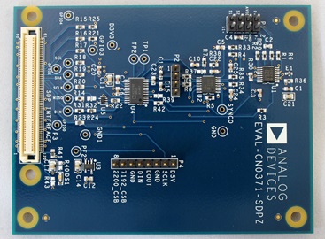
The CN-0371 circuit uses the EVAL-CN0371-SDPZ circuit board and the EVAL-SDP-CB1Z SDP-B controller board. The two boards have 120-pin mating connectors, allowing quick setup and evaluation of the performance of the circuit. The circuit board contains the circuit to be evaluated, and the SDP-B board is used with the CN-0371 Evaluation Software to capture the data from the circuit board.
Equipment Needed
The following equipment is needed:
- A PC with a USB port and Windows® XP (32-bit),Windows Vista®, or Windows 7
- The EVAL-CN0371-SDPZ circuit board
- The EVAL-SDP-CB1Z SDP-B controller board
- The CN-0371 Evaluation Software
- Measurement Specialties, Inc., E-100 Economy Series LVDT (EVAL-CFTL-LVDT)
Getting Started
Download the CN0371.zip file and run the setup.exe file. By default, the program is installed in the Analog Devices directory. The program name is CN0371.
Functional Block Diagram
See Figure 5 for the circuit block diagram. For the complete circuit schematic, see the EVAL-CN0371-SDPZ-Schematic.pdf file, which can be found in the CN-0371 Design Support Package. The 5 V supply for the circuit board is supplied by the USB bus via the SDP-B board 120-pin connector.


Setup
Connect the 120-pin connector on the EVAL-CN0371-SDPZ circuit board to the CON A connector on the EVAL-SDP-CB1Z SDP-B board. Use nylon hardware to firmly secure the two boards, using the holes provided at the ends of the 120-pin connectors.
Test
Launch the evaluation software and connect the USB cable from the PC to the mini-USB connector on the SDP-B board.
When USB communications are established, the SDP-B board can send, receive, and capture data from the circuit board.
Figure 6 shows a photo of the circuit board connected to the SDP-B board. Information regarding the SDP-B board can be found in the UG-277 User Guide.
Information and details regarding test setup, calibration, and how to use the evaluation software for data capture can be found in the CN-0371 Software User Guide.


Connectivity for Prototype Development
The EVAL-CN0371-SDPZ circuit board is designed for use with the EVAL-SDP-CB1Z SDP-B board; however, any microprocessor can be used to interface to the SPI interface of the AD7192. For another controller to be used with the EVAL-CN0371-SDPZ circuit board, software must be developed by a third party.
There are existing interposer boards that can be used to interface to the Altera and Xilinx field programmable gate arrays (FPGAs). The BeMicro SDK board from Altera can be used with the BeMicro SDK/SDP interposer using nios drivers. Any Xilinx evaluation board that features an FMC connector can be used with the FMC-SDP interposer board.
The EVAL-CN0371-SDPZ is also compatible with the Digilent, Imod interface specification.
Figure 6 shows a photo of the system test setup. Complete documentation including schematics, layouts, Gerber files, and bill of materials can be found in the CN0371 Design Support Package at www.analog.com/CN0371-DesignSupport .