ADPL83200
推荐用于新设计Low Loss PowerPath Controller in a ThinSOT Package
- 产品模型
- 1
概述
- Very Low Loss Replacement for Power Supply OR’ing Diodes
- Minimal External Components
- Automatic Switching Between DC Sources
- Simplifies Load Sharing with Multiple Batteries
- Low Quiescent Current: 11μA
- 3V to 28V AC/DC Adapter Voltage Range
- 2.5V to 28V Battery Voltage Range
- Reverse Battery Protection
- Drives Almost Any Size MOSFET for a Wide Zange of Current Requirements
- MOSFET Gate Protection Clamp
- Manual Control Input
- Low Profile (1mm) ThinSOT™ Package
The ADPL83200 controls an external P-channel MOSFET to create a near-ideal diode function for power switchover or load sharing. This permits highly efficient OR’ing of multiple power sources for extended battery life and low self-heating. When conducting, the voltage drop across the Metal-oxidesemiconductor field-effect transistor (MOSFET) is typically 20mV. For applications with a wall adapter or other auxiliary power source, the load is automatically disconnected from the battery when the auxiliary source is connected. Two or more ADPL83200s can be interconnected to allow load sharing between multiple batteries or charging multiple batteries from a single charger.
The wide supply operating range supports operation from one to six Li-Ion cells in series. The low quiescent current (11μA typical) is independent of the load current. The gate driver includes an internal voltage clamp for MOSFET protection.
The STAT pin can be used to enable an auxiliary P-channel MOSFET power switch when an auxiliary supply is detected. This pin may also be used to indicate to a microcontroller that an auxiliary supply is connected. The control (CTL) input enables the user to force the primary MOSFET off and the STAT pin low.
The ADPL83200 is available in a low-profile (1mm) ThinSOT package.
- Cellular Phones
- Notebook and Handheld Computers
- Digital Cameras
- USB-Powered Peripherals
- Uninterruptible Power Supplies
- Logic Controlled Power Switch
参考资料
数据手册 1
用户手册 1
ADI 始终高度重视提供符合最高质量和可靠性水平的产品。我们通过将质量和可靠性检查纳入产品和工艺设计的各个范围以及制造过程来实现这一目标。出货产品的“零缺陷”始终是我们的目标。查看我们的质量和可靠性计划和认证以了解更多信息。
| 产品型号 | 引脚/封装图-中文版 | 文档 | CAD 符号,脚注和 3D模型 |
|---|---|---|---|
| ADPL83200IS6#TRPBF | 6-Lead TSOT-23 |
这是最新版本的数据手册
软件资源
找不到您所需的软件或驱动?
申请驱动/软件工具及仿真模型
LTspice
LTspice中提供以下器件型号:
- ADPL83200
LTspice®是一款强大高效的免费仿真软件、原理图采集和波形观测器,为改善模拟电路的仿真提供增强功能和模型。
评估套件
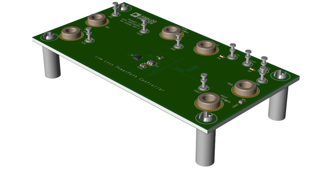
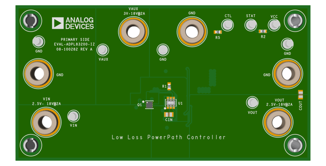
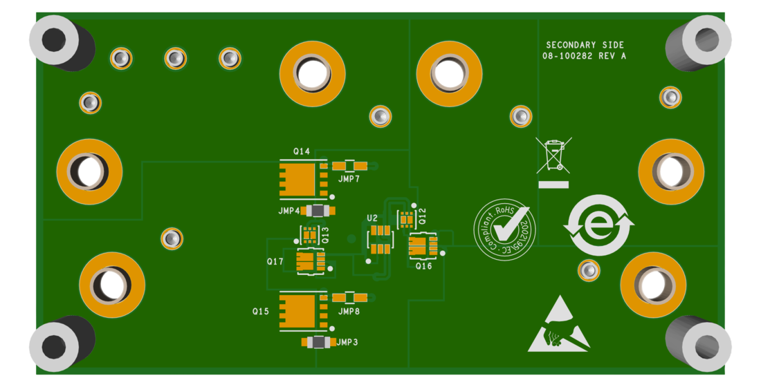
评估:ADPL83200
资料
最新评论
需要发起讨论吗? 没有关于 ADPL83200的相关讨论?是否需要发起讨论?
在EngineerZone®上发起讨论