
温度検出ソリューション
アナログ・デバイセズの幅広い温度検出ソリューションのポートフォリオには、豊富なシグナル・チェーン、集積化センサーtoビット・ソリューション、ディスクリート・テクノロジーなどが含まれ、設計を迅速に開始することができます。
当社の熱電対は小型で堅牢かつ安価です。コスト効率に優れたサーミスタは、温度範囲が-40℃~150℃に限定され、非常に非線形であり、相当なシグナル・コンディショニングを必要とします。測温抵抗体(RTD)は、正確で安定しており、温度範囲が広く、最高水準の精度を確保することができます。シリコン・ベースの温度計測センサーは、線形で安定しており、容易に導入可能で、-55℃~+150℃の狭い温度範囲の測定に最適です。最後に、当社の機能完備の集積化センサーとアナログ・フロント・エンド製品は、設計者に高精度で信頼性の高いビルディング・ブロックを提供し、システム設計を迅速化します。
価値と利点
当社の熱電対は、交換可能かつコンパクトで、-270℃~+1800℃という極端な温度を測定でき、応答時間が短く、自己発熱しません。サーミスタは、低温および高温アプリケーションに最適で、耐久性が高く長寿命であるだけでなく、仕様の温度範囲内で約±0.2℃という高精度も備えています。RTDは、動作温度範囲が-200℃~+850℃で、精度、信頼性、および安定性に優れています。デジタル温度センサーとシリコン・センサーは、容易に導入可能かつ高精度であり、シグナル・コンディショニング不要で優れた精度のデジタル出力を提供する、機能完備のプラグ&プレイ・ソリューションです。


RTD、熱電対、サーミスタ、デジタル、およびシリコン・ベースの温度センサーに最適
温度計測の設計を迅速化するシグナル・チェーンとリファレンス・デザイン・ソリューションを提供
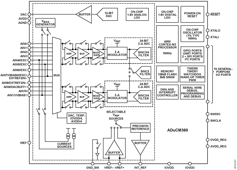
センサーとAFE(アナログ・フロント・エンド)を組み合わせ、システム設計を迅速化するソリューション
ソリューション・リソース
シグナル・チェーン


ハードウェア製品


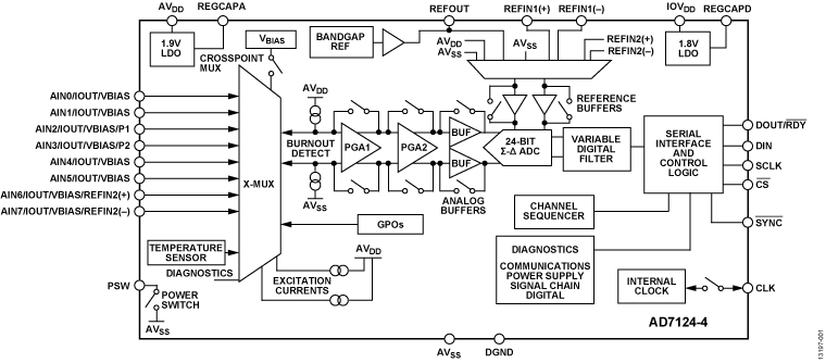
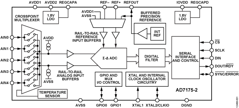
A/Dコンバータ、24ビット、4チャンネル、低ノイズ、低電力、Σ-Δ型、PGA / リファレンス内蔵
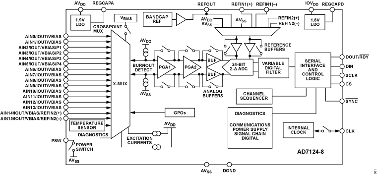
A/Dコンバータ、24ビット、8チャンネル、低ノイズ、低消費電力、Σ-Δ型、PGA / リファレンス内蔵


リファレンス・デザイン
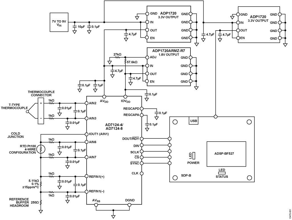

冷接点補償機能付きの低消費電力マルチチャンネル熱電対測定システム
※Rev.Aを翻訳したものです。最新版は英語資料をご覧ください。
冷接点補償機能付きの低消費電力マルチチャンネル熱電対測定システム
※Rev.Aを翻訳したものです。最新版は英語資料をご覧ください。

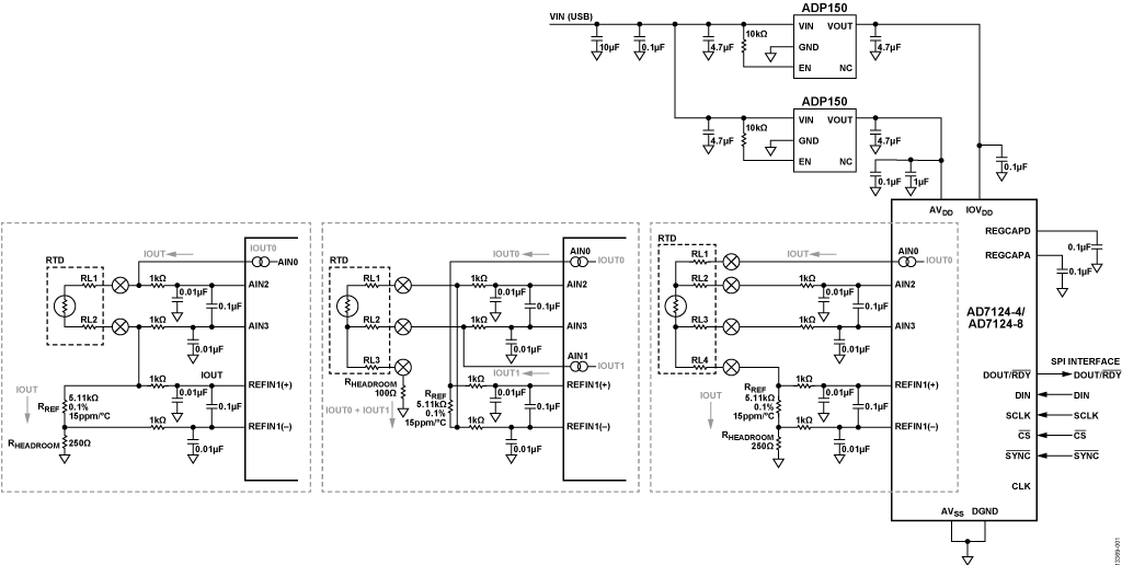
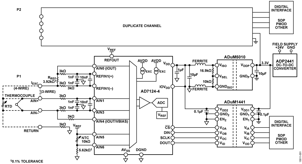
高精度マルチ・チャンネル熱電対測定回路
※Rev.0を翻訳したものです。新ver.は英語資料をご覧ください。
主な資料
CN0172 Software Evaluation User Guide
MT-101 Tutorial: Decoupling Techniques
-

pdf
MT-101: Decoupling Techniques

954 kB
トレーニングおよびサポート
トレーニングおよびチュートリアル
Analog Dialogue
6 1, 2023
モータ用のエンコーダの設計手法、サステナブルな次世代アプリケーションを実現するには?


ビデオ
12 20, 2022
高精度、低消費電力測定装置設計に伴う課題を解決する

ビデオ
9 15, 2022
27:47Solving Low Power Precision Measurement Design Challenges

Analog Dialogue
8 1, 2022
サーミスタをベースとする温度計測システム【Part 2】システムの最適化と評価
Analog Dialogue
7 1, 2022
サーミスタをベースとする温度計測システム【Part 1】 設計上の課題、回路の構成

Technical Articles
3 29, 2017
温度/ビット変換ファミリ製品にカスタム・サーミスタを使用する方法
Analog Dialogue
3 1, 2016
RTDによる温度測定用アナログ・フロントエンドの設計
ファイルおよびダウンロード

{{modalTitle}}
{{modalDescription}}
{{dropdownTitle}}
- {{defaultSelectedText}} {{#each projectNames}}
- {{name}} {{/each}} {{#if newProjectText}}
-
 {{newProjectText}}
{{/if}}
{{newProjectText}}
{{/if}}
{{newProjectTitle}}
{{projectNameErrorText}}