Overview
Design Resources
Design & Integration File
• Schematic• Bill of Materials
• Gerber Files
• Layout Files Download Design Files 1.09 M
Evaluation Hardware
Part Numbers with "Z" indicate RoHS Compliance. Boards checked are needed to evaluate this circuit.
- EVAL-AD7960FMCZ ($140.09) 18-Bit, 5 MSPS, LVDS Data Acquisition System
- EVAL-CN0388-FMCZ ($134.00) Isolated 600 Mbps, LVDS, 18-Bit, Module
- EVAL-SDP-CH1Z ($458.85) Eval Control Board
Features & Benefits
- 18-bit, 5MSPS Data Acquisition System
- Isolated LVDS Output
- 600Mbps Serial Data Capability
Product Categories
Markets and Technologies
Parts Used
Documentation & Resources
-
CN0388: Isolated 600 Mbps, LVDS, 18-Bit, 5 MSPS Data Acquisition System (Rev. 0)9/19/2016PDF489 K
Circuit Function & Benefits
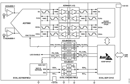
The circuit shown in Figure 1 demonstrates isolation of an analog front end (18-bit, 5 MSPS AD7960 analog-to-digital converter (ADC)) at 600 Mbps using the ADN4651 LVDS isolator. An interposer board with the ADN4651 connects to the standard AD7960 evaluation platform, isolating the analog front end board from the high speed SDP-H1 system demonstration platform (EVAL-SDP-CH1Z). The SDP-H1 contains a Xilinx Spartan 6 FPGA to capture acquisitions and a ADSP-BF527 DSP to communicate with the PC.
Galvanic isolation of external interfaces is required in harsh environments for safety, functionality, or improved noise immunity. This includes analog front ends used in data acquisition modules for industrial measurement and control. Bandwidth requirements for converter interfaces are increasing, as trends such as Industry 4.0 and the Internet of Things (IoT) demand far more ubiquitous measurement and control, with greater speed and precision. This poses a challenge for isolation, because even standard digital isolators are limited to 150 Mbps operation.
For measurement and control applications in industrial environments, the benefits of such an isolated analog front-end implementation include:
- Ease of design due to the drop-in LVDS isolator with fully compliant input/output and ultralow jitter.
- High bandwidth of 600 Mbps to support increased ADC resolution and speed.
- Galvanic isolation for protection from mains voltages, isolated measurement of power supplies, or noise immunity from digital or power supply circuits.
The circuit in Figure 1 demonstrates an industry-leading solution to LVDS isolation at 600 Mbps using the ADN4651 dual-channel isolator.

Circuit Description
The interposer circuit relies upon two ADN4651 600 Mbps LVDS isolators to isolate the LVDS interface to the AD7960. As shown in Figure 1, two LVDS clocks are sent from the Spartan 6 FPGA to the AD7960; the 5 MHz sample clock (CNV±) and a 300 MHz reference clock (CLK±). The AD7960 uses the 300 MHz reference to clock out bursts of sample data at 600 Mbps on D±, synchronous with an echoed 300 MHz clock (DCO±). D± is idle after each data burst to avoid interfering with the acquisition phase of the converter. The ADN4651 houses a pair of bidirectional digital isolators that integrate Analog Devices, Inc., iCoupler® technology to operate at high speed with very low jitter. The VIN+ and VIN− ac voltage inputs are passed through two separate ADA4899-1 unity-gain stable voltage feedback op-amps to which their corresponding outputs are fed into the AD7960. The differential signal of the two input signals then undergoes analog-to-digital conversion and is sent out via D±, synchronized to DCO±.
The Blackfin® ADSP-BF527 outputs the appropriate logic high and logic low levels using 1.8 V logic only through the ADuM4400 quad digital isolators to the AD7960 enable pins (EN0 to EN3), as well as the on-board LDO enable (PC_C2M) and the SDP ID EEPROM address (GA0, GA1). The enable pins on the AD7960 can be configured to specific operational requirements. Full information is available in the AD7960 data sheet. The ADuM2251 dual I2C isolator isolates the SDP ID EEPROM clock (SCL) and data (SDA) from the Blackfin ADSP-BF527 interface.
Communications between the Blackfin ADSP-BF527 and Spartan 6 FPGA to the interposer and measurement circuits are controlled through the USB port on the EVAL-SDP-CH1Z to the evaluation software installed on a PC as shown in Figure 1.
The circuit is powered on the logic and bus side by two 12 V dc supplies, where four supply rails are generated on the EVAL-AD7960FMCZ and three supply rails are generated on the EVAL-CN0388-FMCZ. On the EVAL-AD7960FMCZ, the ADP7104 CMOS LDO produces 5 V, the ADP7102 CMOS LDO produces 7 V, the ADP2300 nonsynchronous step-down regulator produces −2.5 V, and the ADP124 CMOS linear regulator produces 1.8 V. On the EVAL-CN0388-FMCZ, the ADP3335 produces 5 V, the ADP151 linear regulator (2.5 V version) produces 2.5 V, and the ADP151 linear regulator (3.3 V version) produces 3.3 V.
As shown in Figure 1, termination resistors of 100 Ω are fitted on each LVDS input and output of the two ADN4651 isolators at CNV±, CLK±, D±, and DCO± (R11, R12, R13, and R14).
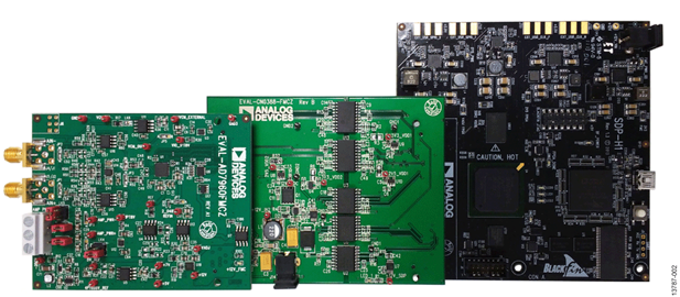
Power and ground on both the logic and bus sides are connected via a barrel connector. Logic levels, clocks, and data signals are connected throughout the EVAL-AD7960FMCZ, EVAL-CN0388-FMCZ, and EVAL-SDP-CH1Z via traces to FMC connectors configured as shown in Figure 2. The ac voltage inputs (VIN+/VIN−) are connected via SMA connectors. An Audio Precision source is an ideal differential driver for the inputs. The user also has the option to apply an external voltage reference to EVAL-AD7960FMCZ via a screw-wire connector.

A complete documentation package including detailed schematics, bill of materials, and layout can be found in the CN-0388 Design Support Package at www.analog.com/CN0388-DesignSupport.
Circuit Evaluation & Test
Before starting evaluation, install the EVAL-AD7960FMCZ evaluation software on a PC. Software installation instructions can be found in the EVAL-AD7960FMCZ User Guide (UG-490).
To begin testing, ensure that the EVAL-AD7960FMCZ, EVAL-CN0388-FMCZ, and EVAL-SDP-CH1Z boards are connected correctly using their FMC connectors. This configuration is shown in Figure 3. To power the EVAL-AD7960FMCZ, EVAL-CN0388-FMCZ, and EVAL-SDP-CH1Z, connect a wall wart power supply to the barrel connectors on the EVAL-CN0388-FMCZ and EVAL-SDP-CH1Z. If the correct voltage levels have been supplied, the +12V_FMC LED (EVAL-AD7960FMCZ), the LED_1 and LED_2 LEDs (EVAL-CN0388-FMCZ), and the FMC_PWR_GD LED (EVAL-SDP-CH1Z) are lit. Alternatively, to test that the circuit is powered correctly, check the voltage levels on the corresponding voltage test points on each board.

Figure 3. Isolated Analog-to-Digital Data Acquisition Test Setup
The labels on each of these test points must match their measured values. On the EVAL-CN0388-FMCZ, there are three voltage test points on each of the isolated and nonisolated sides; +3_3V_SIDE1/SIDE2, +2_5V_SIDE1ADP1/SIDE2, and +12V_IN/IN2. There are four voltage test points on the EVAL-AD7960FMCZ: +7 V, +5 V, +12 V, and VREF.
A complete high speed analog to digital conversion can be tested by connecting differential ac voltage sources through VIN− and VIN+ via the SMA connectors ranging between −VREF and +VREF (after the voltage sources). Acquisition data from the differential input is sent by the EVAL-AD7960FMCZ to the evaluation software installed on the PC. Refer to the EVAL-AD7960FMCZ User Guide (UG-490) for hardware and software operation. Figure 4 shows the Summary tab within the EVAL-AD7960FMCZ evaluation software, which displays a summary of the information gathered.


