MAX77932C
量产8A双相开关电容转换器
用于2S锂电池的业界超高效率、超低IQ的无电感DC-DC转换器,采用小型7mm2 WLP封装
- 产品模型
- 2
概述
- 8A开关电容转换器
- 2S至1S电池电压转换(VOUT = VIN/2)
- 集成电源开关
- 低IQ:工作时30μA,关断时 4μA
- 具有可编程电流和超时的软启动
- 可编程输入过压闭锁
- 可编程输出过压闭锁
- 可编程输出过压闭锁
- 可编程开关频率:0.25MHz至1.5MHz
- 温度警报和保护
- 芯片使能输入
- 电源良好指示器输出
- 频率抖动
- 带中断的I2C接口
MAX77932C是一款独立的双相开关电容转换器,带有集成式电源开关,提供8A输出电流,并将输入电压一分为二。该IC适用于使用2S锂离子电池、同时采用1S级电压为电路供电的应用。此外也适用于从1S电池转向2S电池配置的应用。该IC通过将2S电池电压转换为1S等效输出来简化此类迁移,并让设计人员仍能使用现有的下游1S电源架构。
该IC采用无电感开关电容转换器拓扑,帮助缩小了整体尺寸,并降低了电路的最大高度。其开关频率最高可达1.5MHz,减少了所需的电容的尺寸和数量,从而进一步缩小了解决方案的尺寸。该IC确保能够安全采用集成过压、欠压、过流和热保护,且利用内置的频率扰动功能法度降低了EMI。除了尺寸小巧、更低EMI和保护特性等优势之外,该IC的峰值效率高达98.5%,有助于简化散热设计,非常适合消费电子、医疗和工业领域应用。
该IC具有一个I2C兼容型双线串行接口,由一条双向串行数据线(SDA)和一条串行时钟线(SCL)构成。该IC支持高达3.4MHz的SCL时钟速率。例如OCP、OVLO或UVLO阈值、开关频率、软启动电流和持续时间等转换器参数,都可以通过I2C接口实现轻松调节。该IC在工作时消耗30μA低静态电流,在关断时消耗4μA静态电流。该IC采用微型无铅、0.4mm间距、2.4mm x 2.8mm 42引脚晶圆级封装(WLP)。
应用
- 智能手机和平板电脑
- 超级本电脑
- Chromebook
- DSLR和无反相机
- 移动电源
- 2S锂离子电池应用
- 智能手机直充
- 便携式打印机
- 便携式游戏机
- 移动销售终端(mPOS)设备
- 双向无线电
参考资料
数据手册 1
技术文章 1
视频 2

在线研讨会 1
ADI 始终高度重视提供符合最高质量和可靠性水平的产品。我们通过将质量和可靠性检查纳入产品和工艺设计的各个范围以及制造过程来实现这一目标。出货产品的“零缺陷”始终是我们的目标。查看我们的质量和可靠性计划和认证以了解更多信息。
| 产品型号 | 引脚/封装图-中文版 | 文档 | CAD 符号,脚注和 3D模型 |
|---|---|---|---|
| MAX77932CEWO+ | WLCSP | ||
| MAX77932CEWO+T | WLCSP |
| 产品型号 | 产品生命周期 | PCN |
|---|---|---|
|
6月 30, 2021 - 2143_CANCELLATION DESIGN |
||
| MAX77932CEWO+ | 量产 | |
| MAX77932CEWO+T | 量产 | |
|
5月 24, 2021 - 2143 DESIGN |
||
| MAX77932CEWO+ | 量产 | |
| MAX77932CEWO+T | 量产 | |
这是最新版本的数据手册
软件资源
找不到您所需的软件或驱动?
申请驱动/软件工具及仿真模型
评估套件
MAX77932C评估套件
资料
参考电路
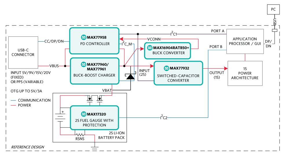


Multicell USB-C PD Charging with Fuel Gauge Platform
使用部分
设计和集成工具
视频
-
 Don't Let a Low Battery Eat Into Your Playtime
最新评论
需要发起讨论吗? 没有关于 MAX77932C的相关讨论?是否需要发起讨论?
在EngineerZone®上发起讨论