LT3669
推荐用于新设计具集成型降压转换器和 LDO 的 IO-Link 收发器
- 产品模型
- 12
概述
- 可兼容 IO-Link® PHY (COM1 / COM2 / COM3)
- 电缆接口保护至 ±60V
- 7.5V 至 40V 工作电压
- 集成型降压开关稳压器
- 最大负载电流:100mA (LT3669) / 300mA (LT3669-2)
- 可同步及可调开关频率范围:250kHz 至 2.2MHz
- 输出电压:0.8V 至 16V
- 集成型 150mA LDO 线性稳压器
- 具可调摆率和电流限值的坚固型线路驱动器
- 采用自适应线路驱动器脉冲方案以安全地开关重负载
- 驱动器可配置为推挽、上拉或下拉
- 可调的上电复位定时器
- 小外形 28 引脚耐热性能增强型 4mm x 5mm QFN 封装
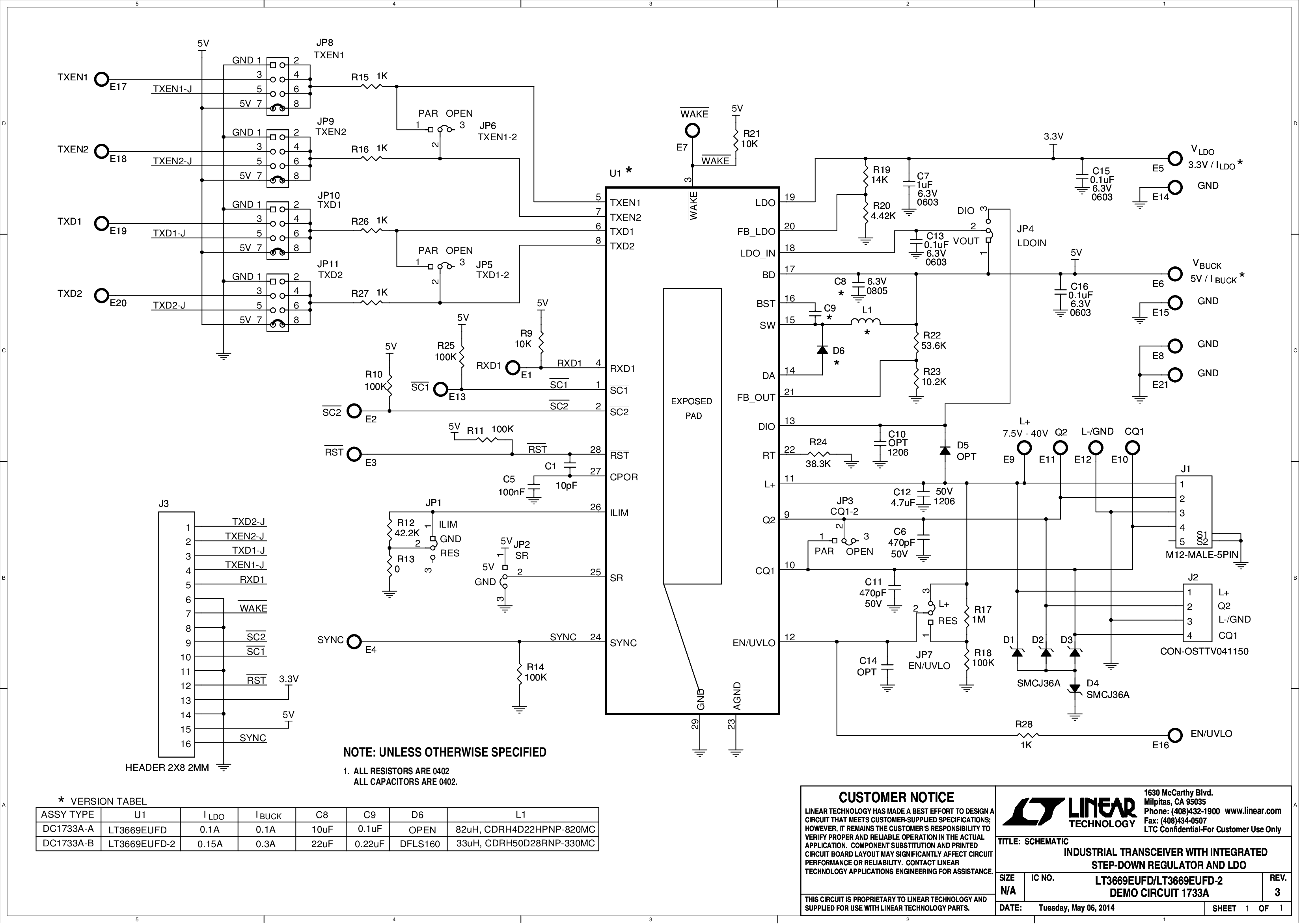
LT®3669 是一款工业收发器,其包含了一个降压型开关稳压器和一个低压差线性稳压器。另外,该器件还内置了唤醒检测功能和一个可编程上电复位定时器。发送器的电流限值和摆率可在外部调节以实现更佳的 EMC 性能。
线路驱动器各能供应 / 吸收高达 250mA的电流,而当连接在一起时则可供应 / 吸收 500mA电流,并且最小残余电压低于 2.1V。由于运用了一种内部自适应脉冲方案,因而使得驱动器能够对重的容性负载和白炽灯泡进行安全的开关操作。热停机功能提供了额外的保护作用。线路接口引脚中的 ±60V 线路保护能力允许使用 L+ 工作电压高达 40V 的标准 TVS 二极管。
在 LT3669 (负载电流高达 100 mA) 中,开关稳压器集成了箝位二极管,而在 LT3669-2 (负载电流高达 300mA) 中则需要一个外部箝位二极管。
LT3669 可实现一个 IO-Link 器件 PHY。对于 IO-Link 主控器设计,请参见 LTC2874 的相关信息。
应用
- 工业传感器和执行器
参考资料
数据手册 1
用户手册 2
技术文章 2
视频 2


新闻 1
解决方案设计及宣传手册 1
产品选型卡 1
ADI 始终高度重视提供符合最高质量和可靠性水平的产品。我们通过将质量和可靠性检查纳入产品和工艺设计的各个范围以及制造过程来实现这一目标。出货产品的“零缺陷”始终是我们的目标。查看我们的质量和可靠性计划和认证以了解更多信息。
| 产品型号 | 引脚/封装图-中文版 | 文档 | CAD 符号,脚注和 3D模型 |
|---|---|---|---|
| LT3669EUFD#PBF | 28-Lead QFN (4mm x 5mm x 0.75mm w/ EP) | ||
| LT3669EUFD#TRPBF | 28-Lead QFN (4mm x 5mm x 0.75mm w/ EP) | ||
| LT3669EUFD-2#PBF | 28-Lead QFN (4mm x 5mm x 0.75mm w/ EP) | ||
| LT3669EUFD-2#TRPBF | 28-Lead QFN (4mm x 5mm x 0.75mm w/ EP) | ||
| LT3669HUFD#PBF | 28-Lead QFN (4mm x 5mm x 0.75mm w/ EP) | ||
| LT3669HUFD#TRPBF | 28-Lead QFN (4mm x 5mm x 0.75mm w/ EP) | ||
| LT3669HUFD-2#PBF | 28-Lead QFN (4mm x 5mm x 0.75mm w/ EP) | ||
| LT3669HUFD-2#TRPBF | 28-Lead QFN (4mm x 5mm x 0.75mm w/ EP) | ||
| LT3669IUFD#PBF | 28-Lead QFN (4mm x 5mm x 0.75mm w/ EP) | ||
| LT3669IUFD#TRPBF | 28-Lead QFN (4mm x 5mm x 0.75mm w/ EP) | ||
| LT3669IUFD-2#PBF | 28-Lead QFN (4mm x 5mm x 0.75mm w/ EP) | ||
| LT3669IUFD-2#TRPBF | 28-Lead QFN (4mm x 5mm x 0.75mm w/ EP) |
这是最新版本的数据手册
硬件生态系统
| 部分模型 | 产品周期 | 描述 |
|---|---|---|
| 接口收发器 1 | ||
| LTC2874 | 量产 | 四通道 IO-Link 主控器热插拔控制器和 PHY |
评估套件
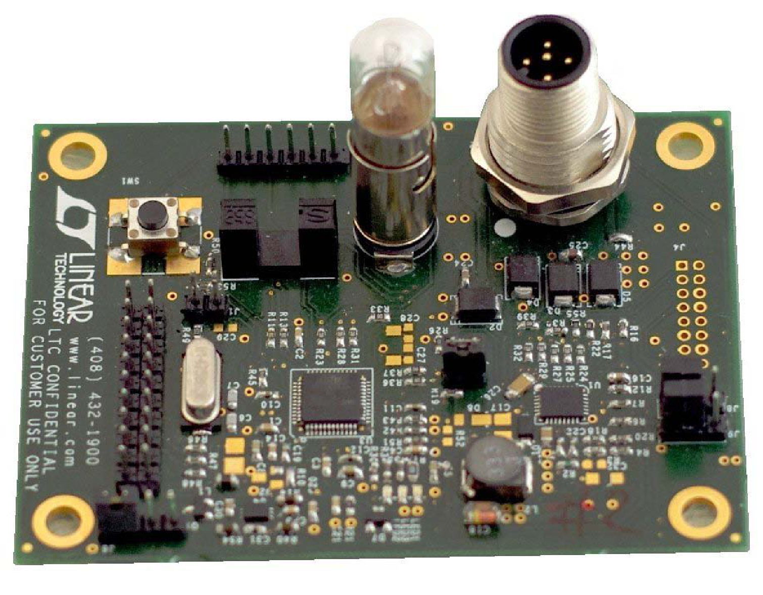
LT3669-1 Demo Board | 7.5V to 40V input with VOUT1 being 5V at 100mA and VOUT2 (LDO) being 3.3V at 100mA
资料
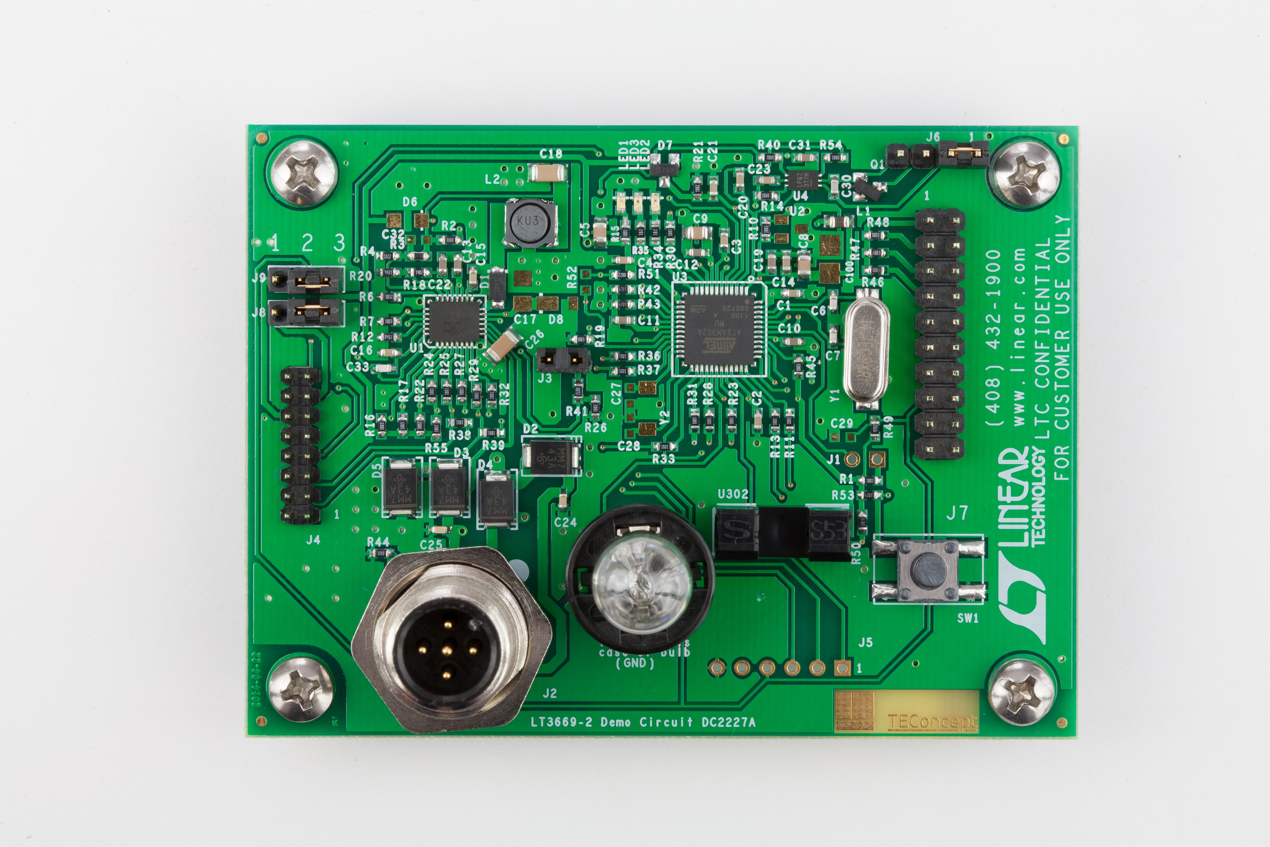
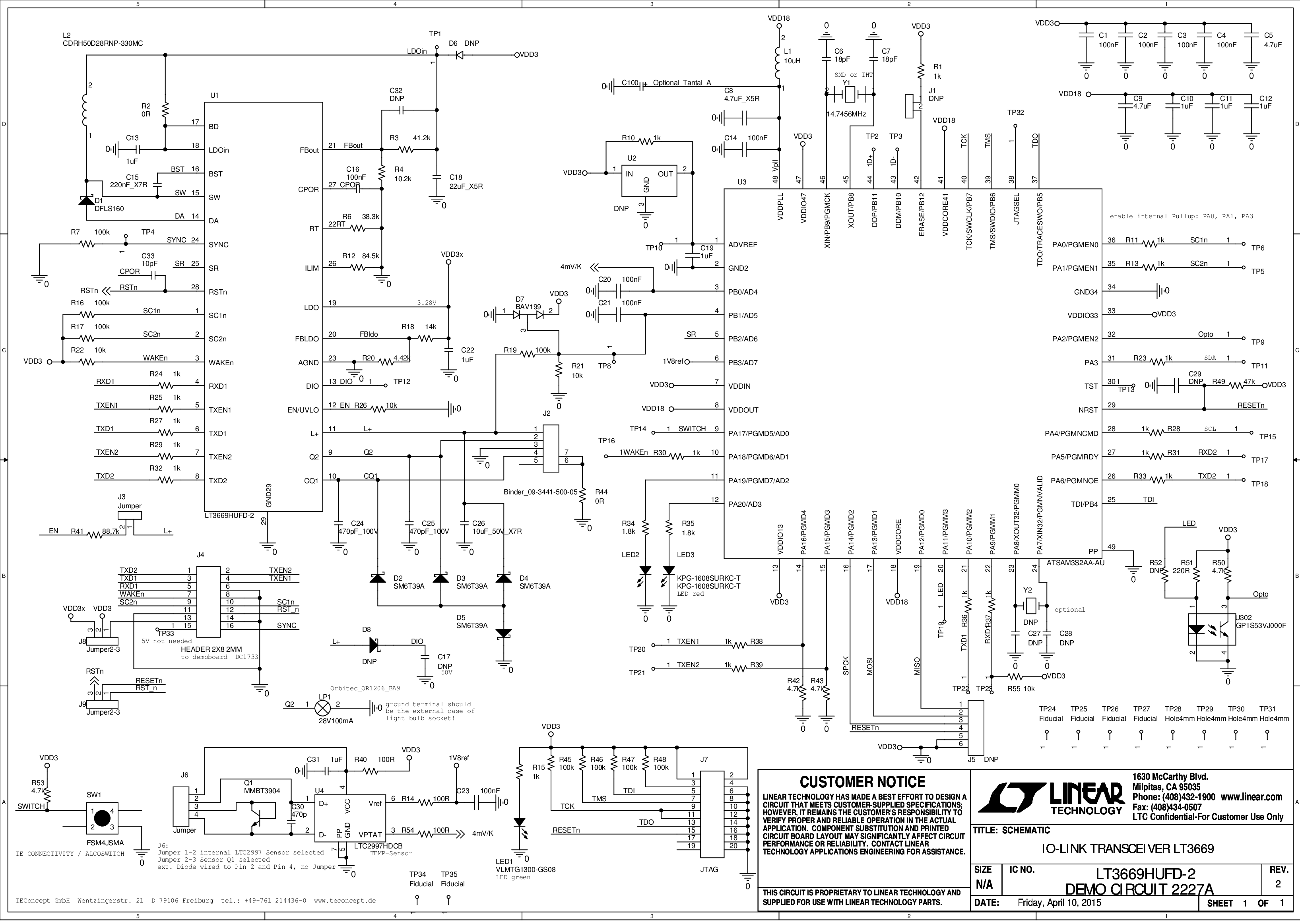
LT3669-2 Demo Board | I/O Link with 18V to 36V Input to 4V at 300mA and 3.3V at 150mA
资料
LT3669-2 Demo Board | 7.5V to 40V input with VOUT1 being 5V at 300mA and VOUT2 (LDO) being 3.3V at 150mA
资料
最新评论
需要发起讨论吗? 没有关于 LT3669的相关讨论?是否需要发起讨论?
在EngineerZone®上发起讨论