CN0363


Overview
Design Resources
Design & Integration File
• Schematic• Bill of Materials
• Gerber Files
• Layout Files (PADS)
• Assembly Drawing Download Design Files 4.42 M
Evaluation Hardware
Part Numbers with "Z" indicate RoHS Compliance. Boards checked are needed to evaluate this circuit.
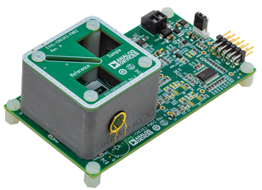
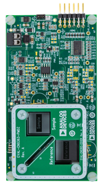
- EVAL-CN0363-PMDZ ($270.71) Dual-Channel Colorimeter with Programmable Gain and Digital Synchronous Detection
Device Drivers
Software such as C code and/or FPGA code, used to communicate with component's digital interface.
AD717x / AD411x IIO Sigma-Delta ADC Linux Driver
AD7173 GitHub Linux Driver Source Code
Features & Benefits
- Dual channel RGB colorimeter
- High sensitivity low noise transimpedance amplifier
- Programmable gain TIA
- Digital synchronous detection
Product Categories
Markets and Technologies
Parts Used
Documentation & Resources
-
EVAL-CN0363-PMDZ User Guide10/16/2018WIKI
Circuit Function & Benefits
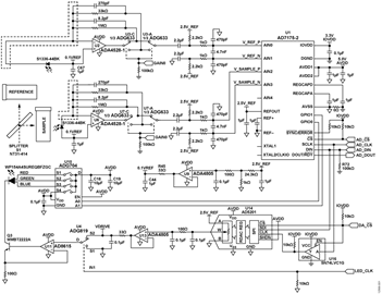
The circuit shown in Figure 1 is a dual-channel colorimeter featuring a modulated light source transmitter, programmable gain transimpedance amplifiers on each channel, and a very low noise, 24-bit Σ-Δ analog-to-digital converter (ADC). The output of the ADC connects to a standard FPGA mezzanine card. The FPGA takes the sampled data from the ADC and implements a synchronous detection algorithm.


By using modulated light and digital synchronous detection rather than a constant (dc) source, the system strongly rejects any noise sources at frequencies other than the modulation frequency, providing excellent accuracy.
The dual-channel circuit measures the ratio of light absorbed by the liquids in the sample and reference containers at three different wavelengths. This measurement forms the basis of many chemical analysis and environmental monitoring instruments used to measure concentrations and characterize materials through absorption spectroscopy.
Circuit Description
A clock set to a user-programmable frequency modulates one of the three LED colors with a constant current driver built around the AD8615 op amp, the ADG819 switch, and the AD5201 digital potentiometer. The beam splitter sends half the light through the sample container and half through the reference container. The ADA4528-1, configured as a transimpedance amplifier, then converts the photodiode current into an output voltage square wave, whose amplitude is proportional to the light transmitted through the sample or reference containers. The transimpedance amplifiers use the ADG633 single-pole, double-throw (SPDT) switches to select one of two transimpedance gains. The AD7175-2 Σ-Δ ADC samples the voltage and sends the digital data to an FPGA for digital demodulation.
The FPGA implements synchronous demodulation by first synchronizing a numerically generated sine wave with the LED clock, and then multiplying this sine wave with the sampled ADC data. In addition, a 90° shifted version of this sine wave is also multiplied with the ADC data to obtain the quadrature component of the modulation signal. The result of these operations are two low frequency demodulated signals representing the in-phase and quadrature components of the received light on each channel, respectively. A narrow FIR low pass filter removes all other frequency components, making it easy to calculate the magnitude and phase shift of the amplitude measured at the photodiodes, while rejecting any light or electrical noise at frequencies different from the LED clock. The ADG704 multiplexer connects the power rail to one of the three LED colors, allowing the user to select the test wavelength through a 2-bit address. The AD8615 and an NPN transistor make up a simple current source, with the LED current given by

where:
VNON-INVERTING is the voltage at the non-inverting input of the AD8615.
REMITTER is the value of the resistor connected to the emitter of Transistor Q3.
The ADG819 SPDT switch is connected to the set point voltage and to ground, and its control pin is connected to the reference clock. As the clock oscillates between high and low, the set point to the current source changes from 0 mA to the desired output current, thereby generating a square wave signal.
The AD5201 digital potentiometer acts as a programmable resistor divider from the 2.5 V reference, allowing 33 different current output settings for the LED current.
Both the sample and reference containers receive one-half of the LED light energy, and absorb different amounts of light depending on the type and concentration of material in each container. The photodiode on the opposite side of each container generates a small current proportional to the amount of light received.
The first stage of each receiver channel consists of an ADA4528-1 op amp configured as a transimpedance amplifier to convert the output current of the photodiode to a voltage. The ADA4528-1 is an auto-zero amplifier resulting in negligible offset, no 1/f noise, and very low broadband noise (5.9 nV/√Hz). Like all auto-zero amplifiers, there is a noise spike at the auto-zero frequency. For the ADA4528-1, the frequency is approximately 200 kHz, but the circuit signal bandwidth rolls off well before then.
The input bias current of the op amp multiplied by the feedback resistor value appears at the output as an offset voltage. The input offset of the op amp voltage appears at the output with a gain dependent on the feedback resistor and the shunt resistance of the photodiode. In addition, any op amp input voltage offset appears across the photodiode, causing the dark current of the photodiode to increase. The ADA4528-1 is therefore ideally suited for this application because of its low offset voltage (2.5 μV).
Figure 2 shows a typical transimpedance amplifier with a single feedback resistor and its ideal transfer function.


Because some solutions under test can have very strong absorption characteristics, it is sometimes necessary to use large feedback resistors to measure the very small currents generated by the photodiode, while at the same time being able to measure large currents corresponding to highly diluted solutions. To address this challenge, the photodiode amplifiers of Figure 1 include two different selectable gains. One gain is set at 33 kΩ, while the other is set at 1 MΩ. Using a single SPDT switch connected to the output of the op amp to switch feedback resistors results in transimpedance gain error due to the on resistance of the ADG633. To avoid this problem, Figure 3 shows a better configuration where the ADG633 switch inside the feedback loop selects the desired resistor, while a second switch connects the next stage of the system to the selected feedback loop. The voltage at the output of the amplifier is

which represents a gain error. However, because one of the ADG633 devices is outside the feedback loop, the output impedance of this stage is the on resistance of the ADG633 (typically 52 Ω), rather than the very low output impedance associated with the output of an op amp in closed-loop operation. The error due to the leakage current of the ADG633 (5 pA typical) is negligible.
Even the best rail-to-rail output amplifiers like the ADA4528-1 cannot swing their output completely to the rails. In addition, the input offset voltage on the ADA4528-1, although very small, can be negative. Rather than including a negative power supply to guarantee that the amplifier never clips, and that it can drive to 0.0 V, an ADA4805-1 op amp provides a buffered 100 mV voltage to bias the anode of the photodiode and the ADA4528-1. The ADA4805-1 is ideally suited as a reference voltage buffer because it maintains unity gain stability when driving large capacitive loads used for decoupling. A second ADA4805-1 is also used to buffer the output of the AD5201 digital potentiometer that sets the LED current.


The output voltage of the photodiode amplifier swings between 0.1 V and 5.0 V. For the 33 kΩ range, the 4.9 V output span corresponds to a full-scale photodiode current of 148.5 μA. For the 1 MΩ range, it corresponds to a full-scale photodiode current of 4.9 μA. When operating in the 1 MΩ gain setting, it is important to shield the photodiode from external light to prevent the amplifier from saturating. Although the synchronous detection scheme described in the following sections strongly attenuates any frequencies that are not synchronous with the LED clock, the detection scheme cannot function properly if the ADC is returning saturated data.
The gain setting for each channel is independently selectable through the FPGA board.
ADC Sampling Rate and Modulation Frequency Selection
The AD7175-2 ADC is configured with the sinc5+sinc1 filter with an output data rate of 250 kSPS to sample both channels with single-cycle settling. This configuration results in an effective sampling rate of 25 kSPS on each channel (data for each channel is output every 40 μs). Any frequencies above 12.5 kHz (such as the odd harmonics of the square wave modulation) alias back into the passband of the ADC; however, the synchronous demodulation stage rejects these frequencies as long as they do not fall right on top of the modulation frequency. To avoid aliases of the modulation waveform folding back into its fundamental, select a modulation frequency according to the following relationship:

where:
FMODULATION is the modulation frequency.
FSAMPLE is the ADC effective output data rate. n is an integer (corresponding to the harmonics of the modulation frequency).
For example, in this system, the effective output data rate is 25 kSPS; therefore, if a modulation frequency of approximately 1 kHz is desired, the frequency must be 1020 Hz (n = 12) or 943 Hz (n = 13) to avoid alias problems. Using this method to select a modulation frequency eliminates the need for sharp anti-aliasing filters on the front end.
Digital Synchronous Detection
Rather than implementing synchronous detection in the hardware (see the Circuit Note CN-0312), this circuit takes the time-sampled data and uses an FPGA to implement digital synchronous detection. Figure 4 shows a representation of the digital synchronous detection block implemented in the FPGA. The FPGA generates the ac excitation signal to drive the LEDs, and a numerically generated sine wave locks to this signal in a digital phase-locked loop. The input signal is multiplied with the digital sine wave and with a 90° shifted version, resulting in two low frequency demodulated signals proportional to the in-phase and quadrature components of the input signal at the modulation frequency. As shown in Figure 4, the magnitude is the root of the sum of the squares of these two components. For more information on this demodulation technique, see the Learn More section.


Power Supplies
The EVAL-CN0363-PMDZ board is powered from an external 6 V to 12 V dc supply. The analog portion of the circuit is supplied by AVDD = 5 V from an ADP7102 low dropout regulator. The digital portion of the circuit is supplied by IOVDD = 3.3 V developed from an ADP1720 low dropout regulator. Alternatively, IOVDD can be supplied from the PMOD connector, VCC, via a link option.
The 2.5 V reference voltage is supplied by the internal 2.5 V reference of the AD7175-2 ADC.
Circuit Performance Measurements
To verify the noise performance of the system, acquire data with all of the LEDs disabled. The synchronous detector still operates at the LED clock frequency, but no light synchronous to this clock is detected; therefore, it removes all dc and ac signals.
Table 1 shows the noise-free bit performance.
| Gain | ADC Output | Final Filtered Output | ||
| Reference Channel ADC | Sample Channel ADC | Reference Channel Output | Sample Channel Output | |
| 1 MΩ | 12.46 | 12.85 | 15.91 | 15.50 |
| 33 kΩ | 15.58 | 15.59 | 18.77 | 18.85 |
| 1 Sample rate = 25 kSPS, excitation frequency = 1020 Hz, output filter bandwidth = 100 Hz. | ||||
Common Variations
Changing the values of the feedback resistors on the photodiode amplifiers changes the amplifier gains, which is an easy way to customize the circuit for a specific application with different light levels. However, the compensation capacitor must also be changed to maintain the same bandwidth and to guarantee that the amplifier is stable.
For systems measuring extremely low levels of light, the cutoff frequency of the synchronous detector’s output low-pass filter can be set to a much lower frequency for the highest performance at the expense of long measurement cycle times.
Because the light output of the LEDs changes with temperature, the system makes measurements as a ratio of the sample and the reference channels. The photodiodes have a gain tolerance of up to ±11%; therefore, even ratiometric variations include some drift as the LED output changes with time and temperature. The addition of an optical feedback network to control the LED light output reduces light variations with temperature and makes possible accurate single-ended measurements.
Rather than modulate the LEDs with a square wave, a DDS or PWM in the FPGA can be used to generate a sine wave modulation. Sine wave modulation reduces the harmonic content of the signal, makes filtering easier, and results in lower noise.
Circuit Evaluation & Test
A complete set of documentation for the EVAL-CN0363-PMDZ board including schematics, layout drawings, Gerber files, and bill of materials can be found in the CN-0363 Design Support Package.
The CN-0363 evaluation software communicates with the FPGA development board to capture and analyze data from the EVAL-CN0363-PMDZ circuit board.
Equipment needed
- EVAL-CN0363-PMDZ circuit evaluation board
- 6 V to 12 V dc, 500 mA power supply or wall wart
- FPGA development board (such as ZedBoard) and a 12 V power supply
- 8 GB SD card, supplied with EVAL-CN0363-PMDZ
- USB keyboard and mouse combination
- HDMI monitor (HD only)
- CN-0363 evaluation software (see the CN-0363 User Guide)
- Distilled water and test liquid samples
Getting Started
Detailed operation of the evaluation hardware and software is available in the CN-0363 User Guide.
HDL software and drivers are provided in the software link to support various FPGA development platforms, such as the Avnet ZedBoard.
The development platforms require an SD card, which is supplied with the CN-0363 hardware. The SD card has been properly partitioned, but must be updated with the latest images. The procedure is described the CN-0363 User Guide.
Functional Diagram
Figure 5 shows a functional block diagram of the test setup.


Setup
Set up the system as follows:
- Connect the PMOD cable between the EVAL-CN0363-PMDZ and the ZedBoard, and connect a 6 V to 12 V dc power supply to the J2 power connector. Do not turn on the supply at this time.
- Connect a USB keyboard/mouse, HDMI monitor, and power supply to the ZedBoard. Do not turn on the supply at this time.
Test
Initialize the system as follows:
- Turn on the power to the EVAL-CN0363-PMDZ board.
- Turn on the power to the ZedBoard.
- Allow the system to boot.
- If needed, enter the appropriate keyboard commands described in the CN-0363 User Guide.
Calibration
The system requires an initial calibration to compensate for misalignment between the LEDs, beam splitter, and photodiodes, as well as to compensate for any mismatch in the response of the photodiodes. To calibrate the system, fill the two containers with distilled water and insert them into the square holes in the PCB. It is also recommended that the photodiodes be shielded from ambient light during the calibration procedure.
Start the automatic calibration procedure in the software; from the Menu bar, open the Calibration dialog box, and click Calibrate. The full calibration procedure process takes a few seconds, and the progress bar indicates the current step. When the calibration is complete, the calibration values are updated. Calibration removes the zero offset and sets the proper gain for each channel. The calibration data also includes a multiplication factor, K, that expresses the relative relationship between the reference and sample channel values at full-scale excitation.
The software calculates the K multiplier for each LED color, so that

where K is the calculated calibration constant.
After performing a calibration, the software uses the calibration constants in all subsequent measurements.
In the field of spectroscopy, absorbance is defined as the logarithmic ratio of the light reaching the material under test to the light transmitted through the material. Beer-Lambert’s law states that the amount of light transmitted through a material decreases exponentially with increasing path length and concentration. By defining absorbance as a logarithm, absorbance is directly proportional to the concentration of the material (given a constant path length).

For a simple way to verify this theory without resorting to harmful chemicals, measure the concentration of dye used for food coloring. Figure 6 shows experimental results from different concentrations of Yellow #5 dye when measured with the EVAL-CN0363-PMDZ.


Yellow solutions strongly absorb blue light; therefore, the measurements were taken using the blue (465 nm dominant wavelength) LED as the source. The x-axis shows the volume concentration (which is in terms of milliliters of dye per milliliter of water, hence unitless), and the y-axis shows the absorbance. As predicted by Beer-Lambert’s law, the absorbance varies linearly with concentration.
Analyzing a Sample
Click the Analyze Sample button in the Automated Data Collection tab (see Figure 7) to perform an automated sample analysis that cycles through all three colors and calculates the absorbance factor for each. The analysis takes a few seconds, and a progress bar is updated to indicate the current step. When the process is complete, the absorbance values are displayed. It is then possible to either try to match the sample to an existing sample from the sample library or to save the sample into the sample library for future use.


Current/Absorbance Measurement and Manual Settings
The Current/Absorbance Measurement tab gives direct manual access to the LED and gain controls, and allows the user to view the raw data (see Figure 8). The following parameters can be set: Excitation Frequency, Excitation Current, LED (Red, Green, or Blue), Reference Channel Gain, and Sample Channel Gain.
If these values are modified, the initial default values can be restored by running the automatic calibration procedure.


Sample Library
The Sample Library tab (see Figure 9) allows the user to manage and compare previously saved sample data. On the left-hand side is a list of all samples. On the right-hand side are the absorbance values for the currently selected samples.
It is possible to select multiple samples by holding down the CTRL key. This feature can be used to directly compare the absorbance of multiple samples to each other. Samples can also be removed from the library by selecting the sample and then clicking Remove. A sample that has been removed from the library cannot be restored.
A photo of the EVAL-CN0363-PMDZ board is shown in Figure 10.


