Overview
Features and Benefits
- Includes schematics, layout, BOM, Gerber files, HDL, Linux® drivers, IIO Oscilloscope, VisualANALOG
- FMC-compatible form factor
- Powered from FMC connector
- Provides two channels of ADC and two channels of DAC with full synchronization capabilities
Product Details
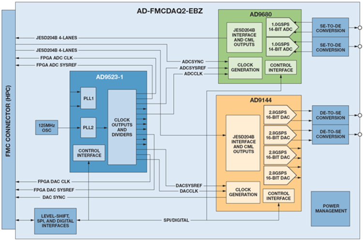
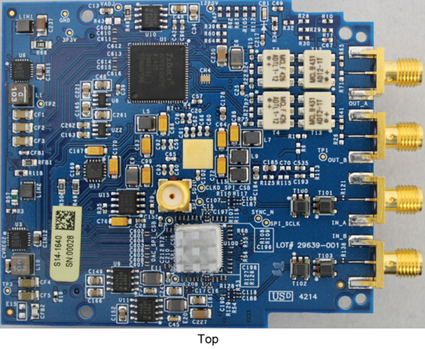
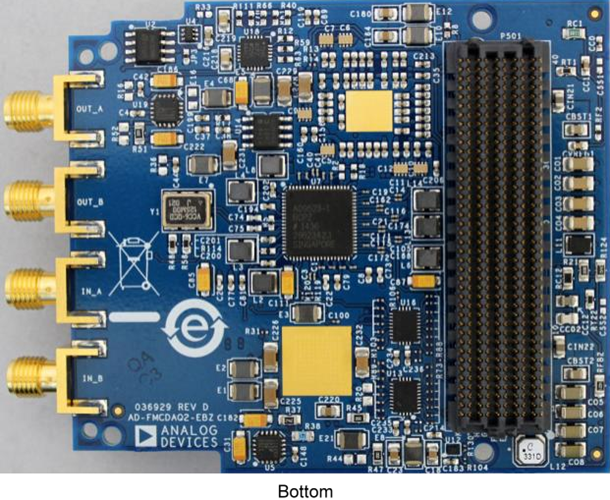
The AD-FMCDAQ2-EBZ module is comprised of the AD9680 dual, 14-bit, 1.0 GSPS, JESD204B ADC, the AD9144 quad, 16-bit, 2.8 GSPS, JESD204B DAC, the AD9523-1 14-output, 1GHz clock, and power management components. It is clocked by an internally generated carrier platform via the FMC connector, comprising a completely self-contained data acquisition and signal synthesis prototyping platform. In an FMC footprint (84 mm × 69 mm), the module’s combination of wideband data conversion, clocking, and power closely approximates real-world hardware and software for system prototyping and design, with no compromise in signal chain performance.Applications
- Electronic test and measurement equipment
- General-purpose software radios
- Radar systems
- Ultra wideband satellite receivers
- Point-to-point communication systems
Markets and Technologies
-
- Body Temperature Measurement Solutions
- Therapy Device Solutions for Healthcare
- Ultrasound Solutions
- Digital X-Ray Solutions
- Computed Tomography Solutions
- Wearable Health Monitor Solutions
- Oxygen Saturation (SpO2) Measurement Solutions
- Respiration Rate Measurement Solutions
- Non-Invasive Blood Pressure (NIBP) Solutions
- Electrocardiogram (ECG) Measurement Solutions
Applicable Parts
Package Contents
- AD-FCMDAQ2-EBZ Board
- 8 GB SD Memory Card
Getting Started
The AD-FMCDAQ2-EBZ module comes with an SD card with the Linux image. All the customer needs is to move the right files from the SD folders to the root based on which FPGA board he is using. Once that is done and the FPGA board is ready to boot of SD card, plug the AD-FMCDAQ2-EBZ module in an HPC FMC slot and turn on the board and they are ready to go.
The advantage of this board is that it has two TX and two RX channels so to start playing around with this demo there is no need for any other equipment other than couple of SMA cables to loop the TX to RX and start seeing the signal in IIO-scope.
Here is the link to our wiki page where customers can find all the info they need for this board:
https://wiki.analog.com/resources/eval/user-guides/ad-fmcdaq2-ebz/quickstart
Reference Board
Reference Board: AD-FMCDAQ2-EBZ
- Product Categories:
- Clock and Timing
- Data Converters
- Interface and Isolation
- Power Management
ADP7104-3.3

High Accuracy 500mA LDO
ADP7104-3.3High Accuracy 500mA LDO
ADP17551.2A Low Vin LDO
ADP17412 A LDO
ADP1740-1.22 A LDO
ADP23844 A Switcher
ADP23844 A Switcher
ADP150Ultra Low Noice 150mA LDO
ADP150Ultra Low Noice 150mA LDO
ADP7104-3.3High Accuracy 500mA LDO
AD9144DAC. 16 bit 2.5 GSPS
ADN4661Buffer
ADN4661Buffer
AD9680ADC 14 bit 1 GSPS
AD72918 CH ADC
AD9523-1Low Jitter Clock Generator

Documentation & Resources
-
AD-FMCDAQ2-EBZ Design & Integration Files3/8/2023ZIP4M
-
AD-FMCDAQ2-EBZ User Guide3/8/2023WIKI
-
Solutions For Rapid Prototyping: Answering the Needs of Practicing Engineers8/23/2023PDF784 K
-
JESD204 Serial Interface2/14/2015
-
 Dual Channel 1GSPS Data Acquisition Kit12/12/2024


