概览
设计资源
评估硬件
产品型号带"Z"表示符合RoHS标准。评估此电路需要下列选中的电路板
- EVAL-CN0566-RPIZ ($2875.00) Phased Array Development Platform
优势和特点
- 10 GHz至10.5 GHz波束控制平台
- 360度相位偏移,分辨率为2.8度
- 31 dB幅度调节范围,分辨率为0.5 dB。
- 8元件线性阵列天线
- 使用PlutoSDR完成数字化
- 直接在树莓派上运行
参考资料
-
Solutions For Rapid Prototyping: Answering the Needs of Practicing Engineers2023/8/23PDF784 K
-
CN0566: Phased Array Development Platform (Rev. 0)2023/4/12PDF1 M
电路功能与优势
Phased array beamforming has been used in radar and communication systems since the mid-20th century. In recent years, these systems have seen extensive adoption in areas such as 5G mobile communications, military and commercial radars, satellite communications, and automotive applications.
Phased array antennas (or beamforming antennas) have an electronically steerable radiation pattern, allowing a robust communication link to be established between two radios. Power from the transmitter can be directed toward the intended receiver, and the receiving antenna can be aimed at the transmitter. In addition, nulls in the receiver's antenna pattern can be placed to reject interfering signals, and a link can be maintained between two radios that are moving with respect to one another. Phased arrays vary widely in complexity, from a few elements in a simple linear array to thousands of elements in planar, cylindrical, conical, and other shaped arrays.
Phased arrays have a steep learning curve, spanning multiple technological and engineering disciplines including microwave RF electronics, continuous and discrete-time signal processing, embedded systems, analog-to-digital and digital-to-analog converters, digital design, and computer networking. Commercial phased array systems are typically expensive and built for a single application, and are not conducive to exploration of basic concepts.
The circuit shown in Figure 1 is a low cost, simplified phased array beamforming demonstration platform that offers a hands-on approach to learning about the principles and applications of phased array antennas. This complete system provides an ideal tool for proof of concept or debugging of more complex systems. It offers the opportunity to explore and understand advanced topics such as beamforming, beam steering, antenna impairments, frequency modulated continuous wave (FMCW) radar, and synthetic aperture imaging. The design consists of RF components, signal processing hardware, and contains an on-board 8-element linear array antenna that operates from 10.0 GHz to 10.5 GHz (X band). This frequency range allows common low cost motion sensor modules to be used as a microwave source.
The circuit is designed to mount directly on a Raspberry Pi, and uses the PlutoSDR low cost software defined radio (SDR) module to digitize the intermediate frequency (IF) output. The software interface is through the Linux industrial input/output (IIO) framework, providing a host of debug and development utilities, and cross-platform application programming interface (API) with Python, GNURadio, and MATLAB support.
Application software can run either locally on the Raspberry Pi or remotely via a wired or wireless network connection. The entire system is powered via a single 5 V, 3 A, USB-C power adapter.
电路描述
Phased array beamforming is a signal processing technique used in antenna arrays for radio communications, radar systems, and medical imaging. Beamforming provides many benefits — the antenna can be aimed directly at a target, which may be a transmitter, receiver, or object being tracked in the case of radar. The antenna pattern's nulls can also be strategically placed to avoid interfering signals.
Forming a beam pattern involves the simultaneous transmission or reception of signals from multiple antennas. A phase shift and gain adjustment is applied to each channel; after which, the individual channels are summed together in either the analog or digital domain, or a hybrid of both. The phase shifters are adjusted to control the direction of the combined radio RF beam, allowing for real-time beam steering and reconfiguration without physically moving the antennas. The main beam width and sidelobe suppression can be adjusted by adjusting the gain (or tapering) the array elements.
The CN0566 main board implements an 8-element phased array, downconverting mixers, local oscillator (LO), and digital control circuitry. The CN0566 outputs are two IF signals at a nominal frequency of 2.2 GHz, that are digitized by a PlutoSDR module.
BEAMFORMING FUNDAMENTALS
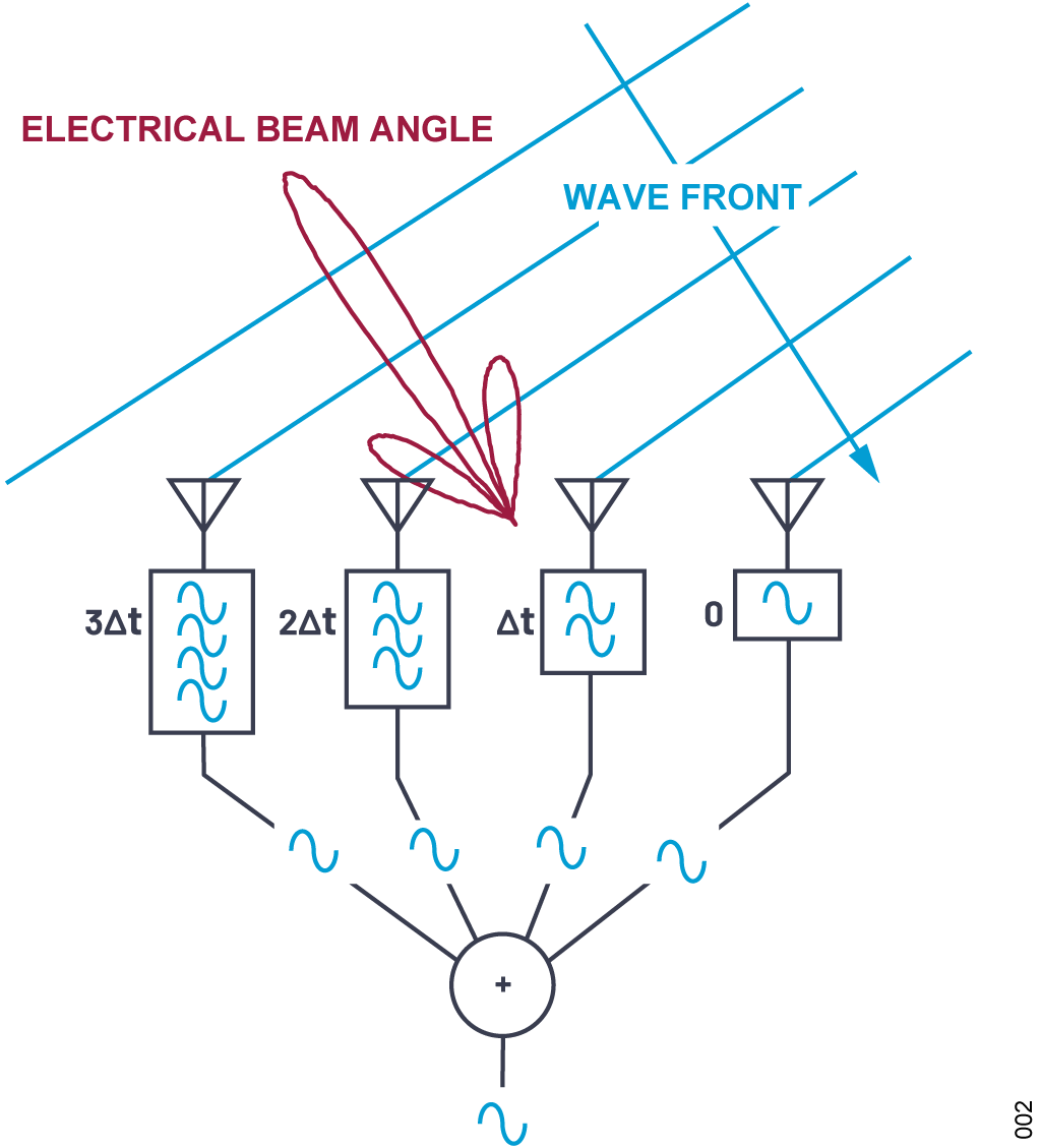
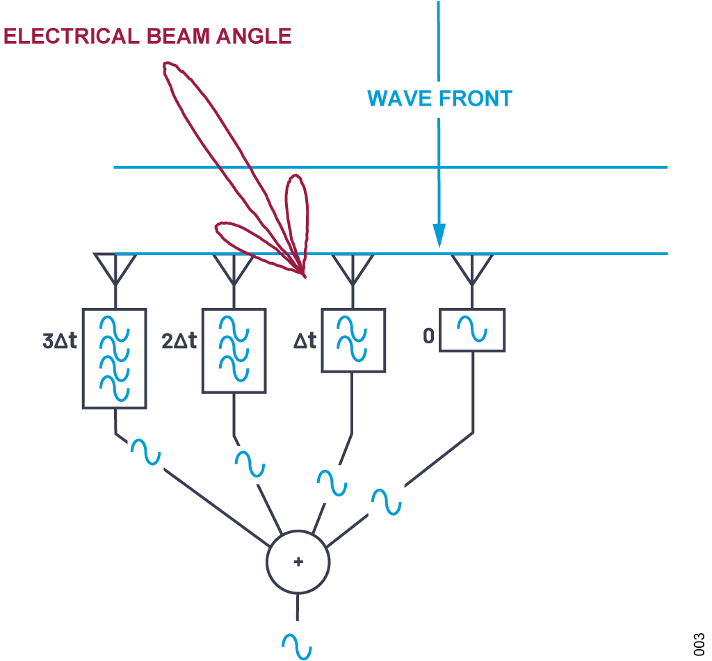
Figure 2 and Figure 3 provide a simple illustration of a wavefront received by four antenna elements from two different directions. The electrical beam is steered 45º to the left, toward the desired transmitter, by inserting time delays in the receive paths, and then summing all four signals together.
In Figure 2, that time delay (configured for a 45º beam) matches the time difference of the wavefront striking each element. In this case, that applied delay causes the four signals to arrive in phase at the point of combination. This coherent combining results in a larger signal at the output of the combiner.
In Figure 3, that same delay is applied; however, in this case, the wavefront from an undesired (interfering) transmitter is perpendicular to the antenna elements. That applied delay misaligns the phase of the four signals, and the output of the combiner is significantly reduced.
In a phased array, time delay is the quantifiable delta needed for beam steering. The time delay to steer the beam is equal to the time it will take for the wavefront to traverse the incremental propagation distance between elements (L). This can best be visualized by drawing a right triangle between the adjacent elements, as shown in Figure 4.
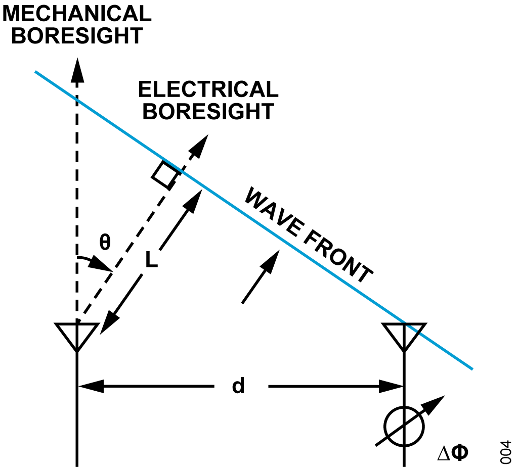
From this drawing, and noting the right angle formed, the value of L can be calculated using Equation 1:

where:
L is the incremental propagation distance between elements.
d is the distance between elements.
θ is the electrical beam angle (angle between mechanical boresight and electrical boresight).
The time delay to steer the beam is equal to the time it will take for the wavefront to traverse that distance, L. Therefore, the time delay is calculated using Equation 2:

where:
Δt is the incremental time delay between elements.
c is the speed of light (3×10⁸ m/s).
Solving for the direction to electrically steer the antenna gives:
θ = sin‐1(Δt c/d)
But time delay can also be emulated with a phase shift, which is common and practical in many implementations. For a narrow bandwidth system, a phase delay can be substituted in for a time delay. That phase delay is simply computed using Equation 3:

where:
ΔΦ is the incremental phase shift between elements.
λ is the signal wavelength.
f is the signal frequency.
Solving for the electrical steering angle, based on the phase shift, gives:
θ = sin‐1 (ΔΦ c / (2 π f d))
As an example, consider two antenna elements spaced 14 mm apart. If a 10.3 GHz wavefront is arriving at 30º from mechanical boresight, then what is the optimal phase shift between the two elements?
θ = 30° = 0.52 rad


ΔΦ = 1.53 rad = 87.4°
So, if the wavefront is arriving at θ = 30º, and then the phase of the neighboring element is shifted by 87.4º, this will cause the individual signals of both elements to add coherently. This maximizes the antenna gain in that direction.
ANTENNA PATTERN FOR A LINEAR ARRAY
In addition to steering angle, it is useful to understand and manipulate the complete antenna gain pattern. The antenna pattern is a combination of the element factor and the array factor. The element factor is the radiating pattern of an element, and it is fixed by the construction of that element. The array factor is the beam pattern that can be electrically controlled by shifting the phase and amplitude of each element.
The array factor is calculated based on array geometry (d for the CN0566's uniform linear array) and beam weights (amplitude and phase). Deriving the array factor for a uniform linear array is straightforward, but the details are best covered in the references cited at the end of this circuit note.
Since the primary concern is how the gain changes with angle, it is often more instructive to plot the normalized array factor relative to unity gain. That normalized array factor can be written as Equation 4:

where:
AF is the normalized array factor.
N is the number of elements.
θ0 is the beam angle.
Since the beam angle, θ0, has already been defined as a function of phase shift between elements ΔΦ; therefore, the normalized antenna factor can also be written as Equation 5:

The conditions assumed in the array factor equation include:
- The elements are equally spaced.
- There is an equal phase shift between elements.
- The elements are all at equal amplitude.
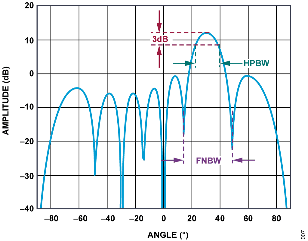
Figure 5 is the array factor for an 8-element array, d = λ/2, θ0 = 30°.
RF DESIGN
Receive Antenna and LNAs
Connecting a receiver to an antenna array is not trivial. At microwave frequencies, cables and connectors must be low-loss and length-matched. The CN0566 eliminates these concerns by including an on-board 8-element patch antenna that operates from 10 GHz to 10.5 GHz as shown in Figure 6.
Each element consists of four sub-elements that are summed equally via printed circuit board (PCB) trace Wilkinson splitters, resulting in a narrowing of the beam pattern in the horizontal direction. A quarter-wavelength shorting stub provides electrostatic discharge (ESD) protection. Each element is capacitively coupled to a 6 GHz to 18 GHz, 24 dB gain ADL8107 low noise amplifier via 10 nF capacitors, and an external antenna can be connected via optional subminiature push-on (SMP) connectors. The LNAs increase the sensitivity of the array, providing a sharp beam pattern even with low power microwave sources.
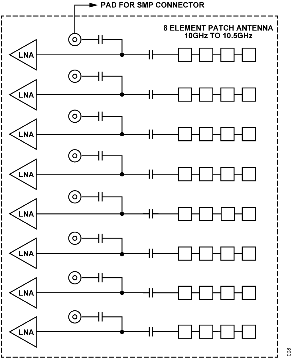
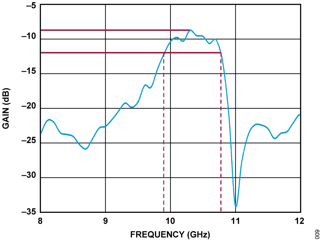
Figure 7 shows the on-board antenna’s gain vs. frequency. The -3 dB bandwidth is 9.9 GHz to 10.8 GHz.
Beamformers
The core of the CN0566 is a pair of ADAR1000 4-channel, 8 GHz to 16 GHz, X band and Ku band beamformers. The ADAR1000 allows per-channel, 360° phase adjustment with 2.8° resolution, and 31 dB gain adjustment with 0.5 dB resolution. The two ADAR1000s are capable of bidirectional, half-duplex operation; however, the CN0566 only connects the ADAR1000 receive paths. The outputs of the ADL8107 LNAs are phase and amplitude shifted by an ADAR1000, and then summed together at its RFIO output as shown in Figure 8.

Local Oscillator/Synthesizer
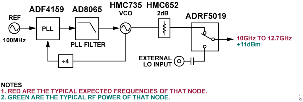
The ADF4159 phase-locked loop (PLL) and the HMC735 voltage-controlled oscillator (VCO) combine to form a frequency synthesizer with a range of 10.5 GHz to 12.7 GHz as shown in Figure 9. This signal is used to drive the LO port of all the mixers. For communications and other fixed-frequency applications, the LO frequency is typically set to 2.2 GHz above the desired signal at the antenna. Therefore, the LO is generally between 12 GHz and 12.7 GHz. The ADF4159 is also capable of generating FMCW ramps or "chirps" for radar applications. The ADF4159 includes a variety of chirp ramp rates and shapes including sawtooth, triangular, and parabolic.
Alternatively, the on-board synthesizer can be disabled, and an external LO can be applied to the LO input SMA connector. This allows the CN0566 to be synchronized to an external radio, or several CN0566 boards to be synchronized to a single LO. Whether generated on-board or externally, the local oscillator is split using monolithic microwave integrated circuit (MMIC) splitter or combiners to the two receive mixers, and to either the on-board transmit path or to an LO output port as shown in Figure 1.
Mixers and Filtering
The RFIO output of the ADAR1000 passes through a 10.6 GHz low pass filter and then enters the RF port of the LTC5548 mixer, as shown in Figure 10.
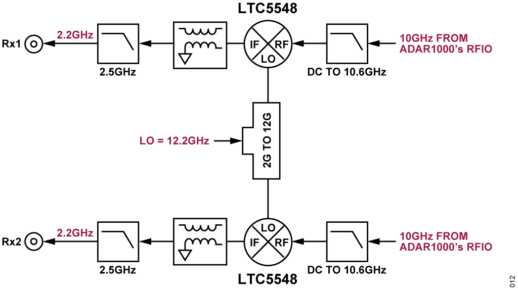
The low pass filter removes the high-side image of the mixer (which in the figure above will appear at 12.2 GHz + 2.2 GHz = 14.4 GHz) as well as any reradiation of the LO (12.2 GHz). The LTC5548 mixer outputs an IF of 2.2 GHz, which is filtered by a 2.5 GHz low pass filter.
Figure 11 shows the measured results of the receive signal path (ADL8107 + ADAR1000 + 10.62 GHz low pass filter + LTC5548 + 2.5 GHz low pass filter). This is for an LO of 12.2 GHz, antenna input of 10 GHz, and an IF of 2.2 GHz. Note that the 12.2 GHz and the 14.4 GHz will be further attenuated by the input bandwidth of the PlutoSDR, resulting in an SFDR of approximately 56 dBc as shown by markers M1 to M4 (-23 dBm + 79 dBm = 56 dBc).
Transmitter Signal Path
While the beamforming section of the CN0566 is receive only, a transmit output is provided for driving an external antenna. For antenna pattern measurements, the antenna can be positioned facing the array at various angles. The frequency of the transmit is known exactly as it is derived from the on-board LO, simplifying digital signal processing. The transmitter can also be used to illuminate a target scene when the CN0566 is used in Doppler and FMCW radar applications.
As shown in Figure 12, the transmitter signal path starts with the transmit input subminiature version A (SMA) connector and outputs to a separate transmit antenna through the two transmit output SMA connectors, TX1 and TX2.

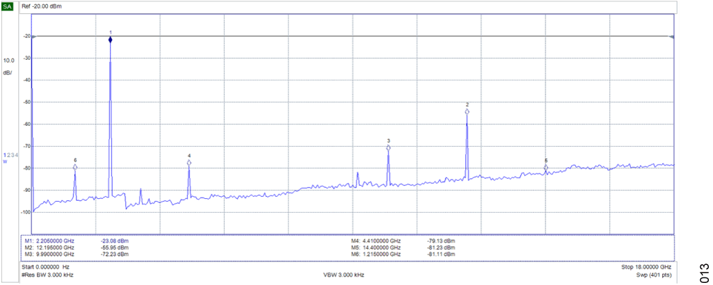
The transmit input is generally the same frequency as the receive IF, which is about 2.2 GHz. This transmit input can either be a continuous wave, modulated communications, or radar signal. Since the output of many SDRs (including that of the PlutoSDR) use a square wave LO, it produces harmonics of the LO frequency. Therefore, the transmit input signal must first pass through a low pass filter. Figure 13 shows the transmit output of the PlutoSDR for a 2.1 GHz tone (without filtering).
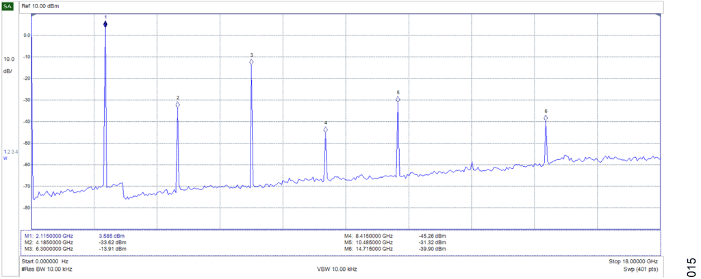
After passing through the 2.5 GHz low pass filter, only the primary signal is visible above the noise floor. This "cleaned up" signal is then fed onto the IF of the LTC5548 and upconverted to 10 GHz to 10.3 GHz.
The 10 GHz to 10.3 GHz RF is then filtered by a 10.6 GHz low pass filter, and amplified by an ADL8107 24 dB LNA, and finally bandpass filtered by a 9.7 GHz to 11.95 GHz filter. Figure 14 shows the mixer output without filtering.
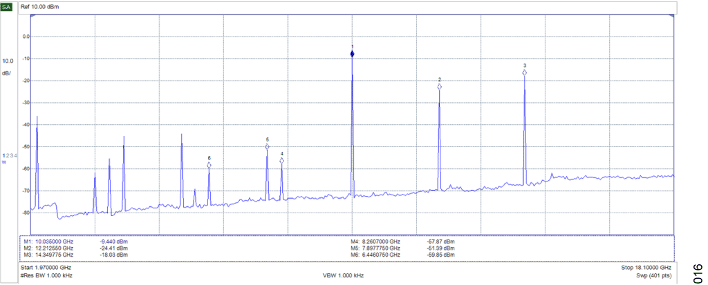
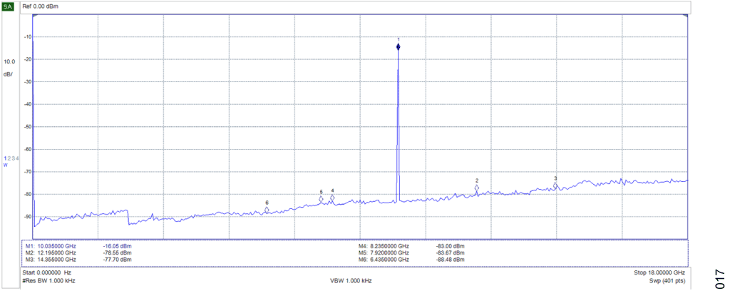
Figure 15 shows the transmit output after amplification and bandpass filtering.
Virtual Arrays
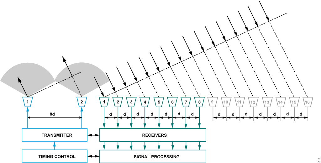
The CN0566 can also be used in virtual arrays, a technique most commonly used in radar systems. In this mode, two transmitter outputs are used, with each transmitter at a different distance from the receive array. As shown in Figure 16, the transmit outputs are toggled at the end of a programmable number of PLL chirps. The data is then combined to create a virtual array that appears to have twice the number of receive elements. Therefore, the receive beam is narrower, but it takes twice the amount of time to gather the data.
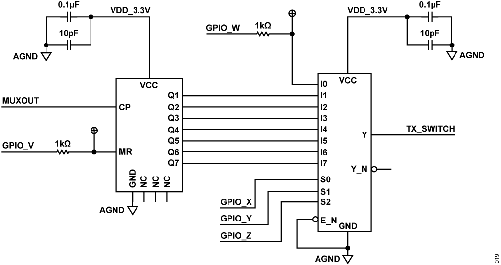
Transmit antenna switching is triggered by the end of a programmable number of PLL chirps. The ADF4159's MUXOUT pin can be programmed to indicate the end of a ramp, and this signal is level-shifted and applied to the clock input of a 7-stage ripple counter, as shown in Figure 17. Three general-purpose input/output (GPIO) signals from the Raspberry Pi drive a data multiplexer inputs, selecting antenna toggle rates of 2, 4, 8, 16, 32, 64, or 128 chirps.
DIGITAL CONTROL AND LEVEL SHIFTING
A Raspberry Pi 4 platform board provides all serial peripheral interface (SPI), I2C, and discrete digital I/O control signals. The Raspberry Pi has logic levels of 3.3 V, which are either used directly or level-shifted to 1.8 V for interfacing with the ADAR1000 and ADF4159. Dual supply level translators are used, with supply pins tied directly to the Raspberry Pi's 3.3 V logic supply and the 1.8 V digital supply. This ensures that the device's digital pins never see a high logic level when not powered.
The ADF4159 MUXOUT also serves as a PLL lock indicator and an end-of-ramp indicator in FMCW modes. A 3.3 V, level-shifted version of MUXOUT drives an LED indicator that shows the PLL lock state.
POWER ARCHITECTURE
The CN0566 derives power directly from a single USB-C receptacle that provides 5 V, 3 A power. This is forwarded to the Raspberry Pi through the 40-pin expansion header, as well as the rest of the on-board power management. Figure 18 shows the complete power tree of the CN0566.
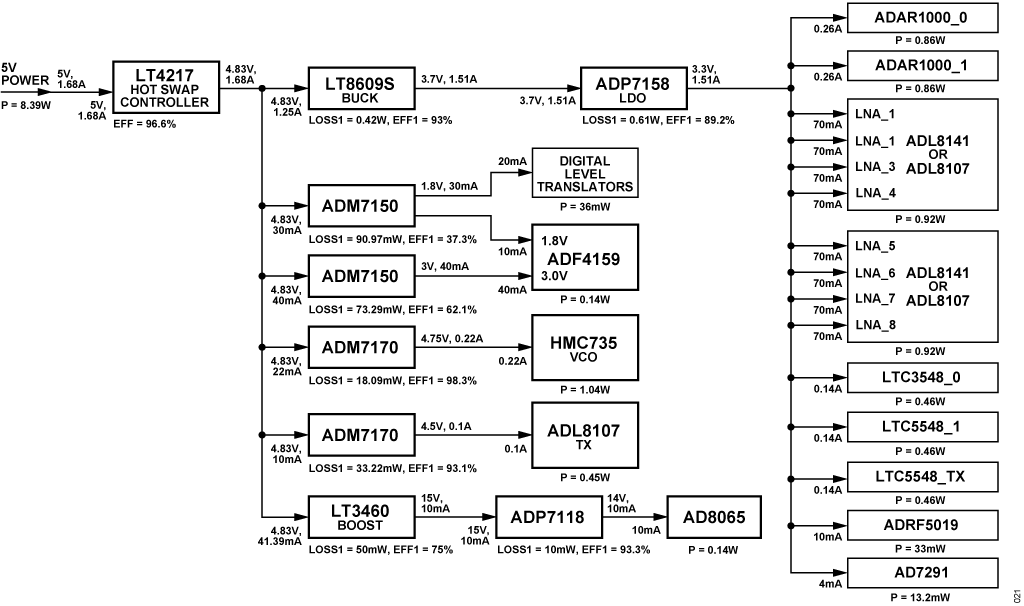
The LTC4217 integrated hot swap controller allows the CN0566 to be safely inserted and removed by limiting the amount of inrush current to the load supply during power-up, and provides a convenient means of measuring the board's power consumption via the IMON output.
The LT8609S is a monolithic constant frequency current-mode step-down DC/DC converter. This device steps down the 5 V input voltage to 3.3 V. This output is then fed into the ADP7158 LDO, which powers the beamformers, LNA, mixers, switches, and ADC at 3.3 V.
The ADM7150 LDO provides the 1.8 V analog supply rail for the digital-level translators and ADF4159.
The ADM7170 is a low quiescent current, low dropout linear regulator that powers the HMC735 VCO. This high output current LDO is ideal for regulation in noise-sensitive applications such as ADC and DAC circuits, precision amplifiers, PLLs/VCOs, and clocking ICs.
The LT3460 step-up DC/DC converter and ADP7118 LDO boost the 5 V input voltage to 15 V, then regulate to 14 V, which is used as the supply of the AD8065 amplifier. It uses a constant frequency, current-mode control scheme to provide line and load regulation. The ADP7118 is a CMOS, low dropout linear regulator that provides high power supply rejection, minimizing synthesizer phase noise.
SYSTEM MONITORING AND CONTROL
The AD7291 8-channel, I2C, 12-bit successive approximation register (SAR) ADC with temperature sensor provides extensive system diagnostics. All supply voltages are monitored, as well as the VCO tuning voltage. The AD7291 input range is 0 V to 2.5 V; resistor dividers scale the measured voltage appropriately. The ADC is placed close to the ADAR1000s, providing an approximate measurement of the board's temperature rise. The measured parameters and scale factors are shown in Table 1.
| AD7291 Input | Parameter | Divider Scale Factor |
| VIN0 | 1.8 V supply | 2 V/V |
| VIN1 | 3.0 V supply | 2 V/V |
| VIN2 | 3.3 V supply | 2 V/V |
| VIN3 | 4.5 V supply | 4.01 V/V |
| VIN4 | Supply of AD8065 amplifier | 7.98 V/V |
| VIN5 | Input voltage | 4.01 V/V |
| VIN6 | Current monitor output of LTC4217 | 1 A/V |
| VIN7 | Control voltage and modulation input of HMC735 | 7.98 V/V |
SYSTEM PERFORMANCE
Ideally, a beamforming array produces a beam that is aimed at a desired angle and has a shape that is as close as possible to the theoretical for a given element taper. For example, setting every element to the same gain, with no phase shift, produces a beam aimed at 0° (mechanical boresight), with a SIN(X)/X or SINC1 profile. Reducing the gain of the outer elements in a triangular profile produces a SINC2 profile, and applying progressively increasing phase shifts across the elements steers the beam away from mechanical boresight.
The ability to produce an accurate beam depends on the ability to accurately set the gain and phase of each element. The CN0566 includes several sources of both gain and phase error that cannot be avoided:
- Mismatch in the elements themselves (likely the smallest error source).
- The ADAR1000's own gain and phase errors.
- A mismatch between the two ADAR1000 devices.
- A mismatch between the two receive paths, including LO splitter, mixers, filters, and other passive components.
- A mismatch between the receiver channels (PlutoSDR or other SDR modules).
System Calibration
Since these errors cannot be avoided, the CN0566 software includes a calibration script. Either an external microwave source or the on-board transmit output connected to an antenna, is placed at mechanical boresight approximately 1 meter from the array. The calibration script then runs through the following operations: Measure and compensate transmit channel mismatch. This ensures that as much of the ADAR1000s' 7-bit gain control is available for accurately tapering the beam rather than compensating for transmit channel mismatch. The procedure is as follows:
- Set all ADAR1000-0 channels to zero phase, mid-scale gain; set all ADAR1000-1 channels to minimum gain. Measure RF signal strength for receive channel zero. Repeat with ADAR1000-0 set to zero gain.
- Calculate how many decibels to increase the gain of the lower of the two receive channels such that the average mismatch is minimized.
- Store these values to the channel calibration file.
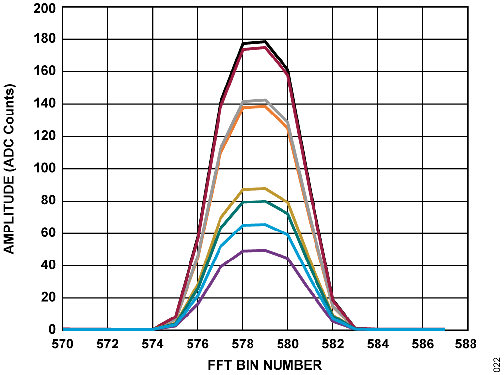
Figure 19 shows the signal-relative signal strengths of each element in the array prior to compensation. The maximum mismatch between elements is 11.2 dB. Note that the strengths are qualitatively in two groups of four elements, indicating a mismatch between the two channels.
Next, measure and compensate for the residual mismatch between element gains by following these steps:
- Set element 0 to maximum gain, and all other elements to minimum gain. Measure the RF signal strength.
- Repeat for the remaining elements, setting one element to the maximum, the rest to a minimum. Measure the RF signal strength.
- Locate the element with the minimum gain. Calculate how much the other elements' gains must be reduced to match that of the minimum element.
- Normalize the reduction factors to unity such that the desired beam taper can be multiplied by the reduction factors.
- Store these values in the gain calibration file.
Figure 20 shows the signal strengths after calibration, with a maximum mismatch of 0.51 dB.
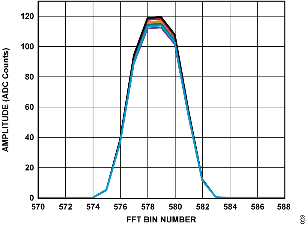
Next, measure and compensate for the phase mismatch between adjacent elements by following these steps:
- Set element 0, 1 to maximum gain, accounting for channel and gain calibration factors.
- Set element 0 to zero phase, then step element 1 phase from 0 to 360º, measuring signal strength at each step.
- Phases are matched when the signal strength is maximized. However, it is much easier to locate the null when the elements are 180° out-of-phase.
- Add 180° to the null phase. This is the phase that must be added to element 1 to compensate for its phase mismatch.
- Repeat for adjacent pairs of elements (1-2, 2-3, 3-4, etc.).
- Start with zero compensation for element 0 and add successive adjacent element compensation values, resulting in a list of values that can be applied to the entire array.
- Store these values in the phase calibration file.
Figure 21 shows the gain vs. phase difference between adjacent elements. Ideally, all nulls would be at ±180°.
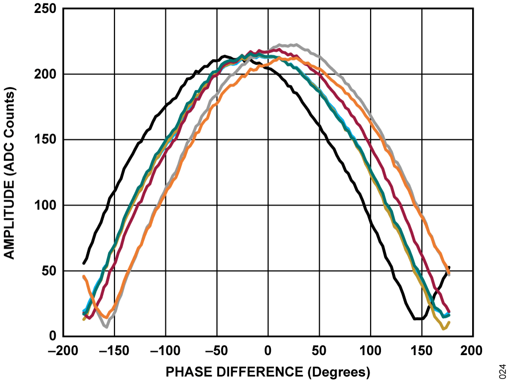
After calibration, gain and phase accuracy across the array approaches the resolution of the ADAR1000 itself, which is better than 0.5 dB with an adjustment range of 31 dB, and 2.8°, respectively.
常见变化
The CN0566 can be extended in the horizontal (azimuth) direction by stacking additional boards side-by-side, allowing a narrower beam to be produced. A common LO must be used across all boards, and an SDR receiver with two synchronized inputs per board must be used to digitize the IF outputs.
If monopulse tracking and hybrid beamforming are not required, the outputs of two or more ADAR1000s can be combined with a passive combiner and digitized by a single-channel ADC (such as the single RX input on a PlutoSDR).
An external, 8-element antenna can be used with the CN0566 via optional SMP RF connectors. Any frequency plan that falls within approximately 8 GHz to 14 GHz operating range can be implemented, changing the on-board splitters, low pass, and band-pass filters accordingly.
For half-duplex (transmit and receive) applications, the ADTR1107 is a 6 GHz to 18 GHz RF front-end. This device incorporates an 18 dB gain, 2.5 dB noise figure receive LNA, and a 25 dBm PSAT transmit amplifier with 22 ns switching speed between transmit and receive.
The ADAR1000EVAL1Z X/Ku phased array reference design is a 32-channel, half-duplex beamforming front-end that includes an antenna with 10 GHz lattice spacing. When coupled with an ADXUD1AEBZ up/down converter board, an EVAL-AD9081 mixed front-end evaluation board and a supported FPGA development platform, fully functional radar and communication systems can be prototyped.
The ADAR3000 and ADAR3001 are 16-channel beamformers for the 17 GHz to 22 GHz and 27.5 GHz to 31 GHz applications, respectively. These devices can be configured for either transmit or receive, and implement a time delay (rather than phase adjustment), eliminating beam squint in wideband applications.
The ADAR4002 single-channel, bidirectional beamformer with a frequency range of 0.5 GHz to 19 GHz. This device includes a programmable time delay from 0 ps to 508 ps (4 ps resolution) or 0 ps to 254 ps (2 ns resolution), and 6-bit attenuation with 0.5 dB resolution.
电路评估与测试
This section covers the setup and procedure for evaluating the EVAL-CN0566-RPIZ. For complete setup details and other important information, refer to the CN0566 User Guide.
EQUIPMENT NEEDED
- CN0566 Kit including:
- EVAL-CN0566-RPIZ with attached Raspberry Pi 4 and PlutoSDR
- USB to micro-USB cable
- SD card with Analog Devices, Inc. Kuiper Linux image
- 5 V, 3 A, USB-C wall adapter
- 10 GHz microwave source (motion sensor)
- Tripod
For Running scripts locally on the Raspberry Pi
- Display monitor with HDMI
- Micro-HDMI to HDMI cable
- USB keyboard and mouse
For running scripts on a remote host computer
- Windows, Linux, or Mac computer with MATLAB or Python IDE
- Ethernet cable
GETTING STARTED
Configure the SD Card with Kuiper Linux for the CN0566 by following the instructions in the CN0566 User Guide. Insert the SD card into the Raspberry Pi's SD card slot.
SETUP AND TEST
Refer to the connection diagram shown in Figure 22.
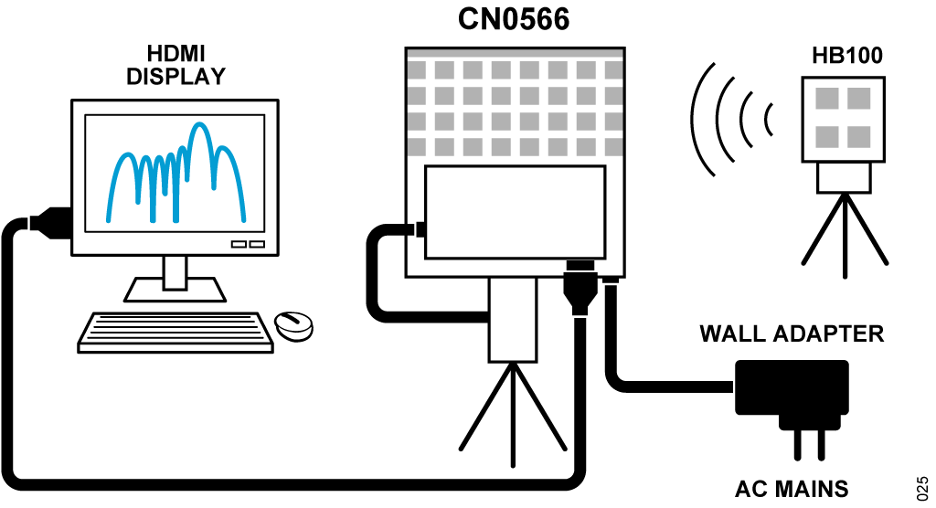
- Connect the PlutoSDR's center micro-USB connector to one of the Raspberry Pi USB ports using the supplied cable.
- Carefully thread the tripod into the tripod mount.
- Plug the USB-C wall adapter into the USB-C power jack on the EVAL-CN0566-RPIZ.
- Power up the microwave source with two AA cells or a 3 Volt power supply. Aim the source at the antenna array.
To run Python examples directly on the Raspberry Pi:
- Connect the Raspberry Pi HDMI output closest to the power connector to the monitor via an HDMI cable.
- Connect the USB keyboard and mouse to the Raspberry Pi USB ports.
- Open a terminal and run the cn0566_find_hb100.py script
- Verify that the spectrum plot shows a single, prominent tone. Type "y", then <enter> to save the frequency.
- Open the cn0566_gui.py script and click the RUN button. In the GUI screen, click the "Auto Refresh Data" check box, then the "Acquire Data" button. Observe the beam pattern.
To run MATLAB examples on a host computer:
- Connect the Windows, Mac, or Linux host computer to the Raspberry Pi with the the Ethernet cable.
- Open MATLAB and run the phaser_hb100_scan.m script.
- Run the phaser_rxtx.m script and observe the beam pattern.


