LTC3204
量产采用 2 x 2 DFN 封装的低噪声稳压充电泵
- 产品模型
- 8
概述
- 固定的 3.3V 或 5V 输出
- VIN 范围:
- 1.8V to 4.5V (LTC3204-3.3/LTC3204B-3.3)
- 2.7V to 5.5V (LTC3204-5/LTC3204B-5)
- 输出电流:
- 高达 150mA (LTC3204-5 / LTC3204B-5)
- 高达 50mA (LTC3204-3.3 / LTC3204B-3.3)
- 具 IQ = 48µA 的自动突发模式 (Burst Mode®) 操作 (LTC3204-3.3 / LTC3204-5)
- 在一般负载条件下均执行恒定频率操作 (LTC3204B-3.3 / LTC3204B-5)
- 低噪声恒定频率 (1.2MHz) 操作
- 内置软启动功能电路可减小浪涌电流
- 停机功能使负载与输入断接
- 停机电流 < 1µA
- 短路保护 / 热保护
- 采用外形扁平的 6 引脚 DFN 封装
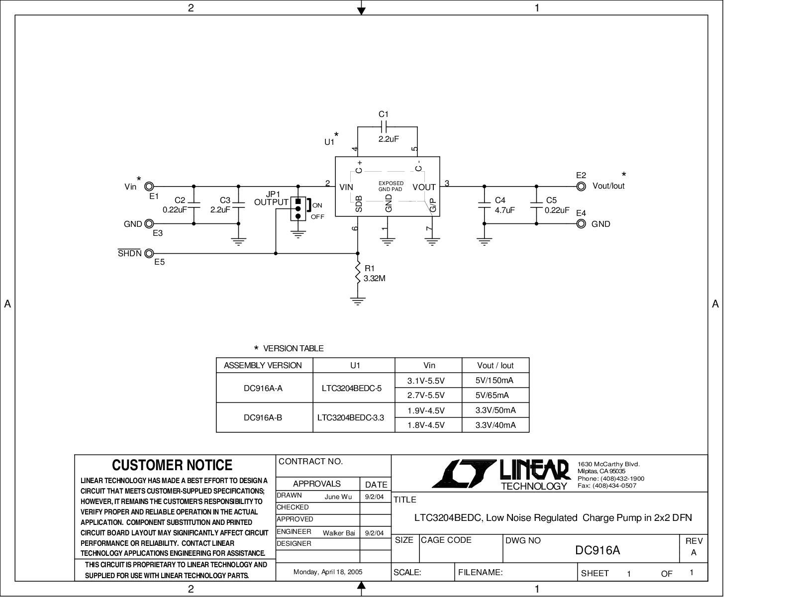
LTC®3204-3.3 / LTC3204-5 / LTC3204B-3.3 / LTC3204B-5 是低噪声、恒定频率 (1.2MHz) 开关电容电压倍增器。LTC3204-3.3 / LTC3204B-3.3能够采用一个 1.8V (两节碱性电池) 的最小输入电压产生一个 3.3V 的稳定输出电压,而 LTC3204-5 / LTC3204B-5 则能依靠一个 2.7V (锂离子电池) 的最小输入产生 5V 输出电压。
LTC3204-3.3 / LTC3204-5 在轻负载时执行自动突发模式 (Burst Mode®) 操作以保持低电源电流,而 LTC3204B-3.3 / LTC3204B-5 则在任何负载条件下均执行恒定频率操作。内置的软启动电路可防止在启动期间产生过大的浪涌电流。热停机和电流限制电路使得这几款器件能安然经受从 VOUT 至 GND 的持续短路。
高开关频率允许使用纤巧型陶瓷电容器,因而较大限度减小了总体解决方案占板面积。在停机模式中,负载与 VIN 断接,而且静态电流减低至 <1µA。LTC3204-3.3 / LTC3204-5 / LTC3204B-3.3 / LTC3204B-5 采用外形扁平 (仅高 0.75mm) 的 6 引脚 2mm x 2mm DFN 封装。
应用
- 两节 AA 电池至 3.3V
- 锂离子电池至 5V
- USB On-The-Go 设备
- 白光 LED 驱动器
- 手持式设备
参考资料
数据手册 1
用户手册 2
ADI 始终高度重视提供符合最高质量和可靠性水平的产品。我们通过将质量和可靠性检查纳入产品和工艺设计的各个范围以及制造过程来实现这一目标。出货产品的“零缺陷”始终是我们的目标。查看我们的质量和可靠性计划和认证以了解更多信息。
| 产品型号 | 引脚/封装图-中文版 | 文档 | CAD 符号,脚注和 3D模型 |
|---|---|---|---|
| LTC3204BEDC-3.3#TRMPBF | 6-Lead DFN (2mm x 2mm w/ EP) | ||
| LTC3204BEDC-3.3#TRPBF | 6-Lead DFN (2mm x 2mm w/ EP) | ||
| LTC3204BEDC-5#TRMPBF | 6-Lead DFN (2mm x 2mm w/ EP) | ||
| LTC3204BEDC-5#TRPBF | 6-Lead DFN (2mm x 2mm w/ EP) | ||
| LTC3204EDC-3.3#TRMPBF | 6-Lead DFN (2mm x 2mm w/ EP) | ||
| LTC3204EDC-3.3#TRPBF | 6-Lead DFN (2mm x 2mm w/ EP) | ||
| LTC3204EDC-5#TRMPBF | 6-Lead DFN (2mm x 2mm w/ EP) | ||
| LTC3204EDC-5#TRPBF | 6-Lead DFN (2mm x 2mm w/ EP) |
这是最新版本的数据手册
软件资源
找不到您所需的软件或驱动?
申请驱动/软件工具及仿真模型
LTspice 2
- LTC3204-5 Demo Circuit - Low Noise Regulated Charge Pump (2.7-5.5V to 5V @ 150mA)
- LTC3204-3.3 Demo Circuit - Low Noise Regulated Charge Pump (1.8-4.5V to 3.3V @ 50mA)
LTspice中提供以下器件型号:
- LTC3204-3.3
- LTC3204-5
- LTC3204B-3.3
- LTC3204B-5
LTspice®是一款强大高效的免费仿真软件、原理图采集和波形观测器,为改善模拟电路的仿真提供增强功能和模型。
评估套件
LTC3204BEDC-3.3 Demo Board | Low Noise Regulated Charge Pump in 2x2 DFN, VIN = 1.8V to 4.5V, VOUT = 3.3V/(40 to 50mA Max)
资料

LTC3204EDC-3.3 Demo Board | Low Noise Regulated Charge Pump in 2 × 2 DFN, Burst Mode, VIN = 1.8V to 4.5V, VOUT = 3.3V/(40mA to 50mA Max)
资料
LTC3204EDC-5演示板 | 采用2x2 DFN封装的低噪声稳压电荷泵,突发模式,VIN = 2.7V–5.5V,VOUT = 5V/(65–150mA)
资料
LTC3204BEDC-5 Demo Board | Low Noise Regulated Charge Pump 2x2 DFN, VIN = 2.7V to 5.5V, VOUT = 5V/(65 to 150mA Max)
资料
最新评论
需要发起讨论吗? 没有关于 LTC3204的相关讨论?是否需要发起讨论?
在EngineerZone®上发起讨论