

ADuM3250
推荐用于新设计Isolated, Half-Bridge Gate Driver with Adjustable Dead Time, 10A Output
- 产品模型
- 6
概述
- 10A peak current (< 1.1Ω RDSON_x)
- Precise timing characteristics
- 41ns max propagation delay over specified temperature range
- 6.3ns maximum channel-to-channel matching
- High common-mode transient immunity (CMTI): >210kV/μs
- 4.5V to 28V driver side supply voltage
- Multiple UVLO options for driver side supplies:
- Grade A: 4.5V maximum
- Grade B: 7.6V maximum
- UVLO VDD1 positive going threshold: 2.25V maximum
- Adjustable dead time control
- CMOS input logic levels
- High junction temperature operation: 150°C
- Safety and regulatory approvals
- UL1577
- VISO = 3000VRMS for 1 minute
- EN/IEC 62368-1
- EN/IEC 61010-1
- IEC 60747-17 (VDE 0884-17) (pending)
- VIORM = 1200Vpeak
- GB4943.1
- 16-lead, RoHS compliant, SOIC_N package (4.0mm creepage)
The ADuM3250 is a 10A isolated, dual channel/half bridge gate driver that employs Analog Devices, Inc., iCoupler® technology to provide a precision timing across the isolation barrier.
Thanks to its strong gate driver capability and precise timing performance, the ADuM3250 is ideal for applications using insulated- gate bipolar transistors (IGBTs) and metal-oxide semiconductor field effect transistors (MOSFETs), as well as wide-bandgap devices such as silicon carbide (SiC) and gallium nitride (GaN) switches, with a maximum recommended switching frequency of up to 1MHz. ADuM3250 provides 1200VPK isolation and comes with small outline integrated circuit (SOIC)-16 package with 4.0mm creepage.
The ADuM3250 secondary side supplies (VDDA, VDDB) support up to 28V. To ensure compatibility and optimal performance across different power switches technologies, ADuM3250 is available in two different undervoltage lock-out (UVLO) options on VDDA and VDDB.
Additional features include a DISABLE pin, which can force the output to a low state, and a dead-time control pin (DT) that prevents simultaneous activation of both channels, thereby avoiding shoot-through conditions.
APPLICATIONS
- IGBT, SiC, GaN applications
- AC-DC and DC-DC power supplies
- Uninterruptable power supplies (UPS)
- Industrial motor drives
- Industrial inverters
参考资料
数据手册 1
用户手册 1
ADI 始终高度重视提供符合最高质量和可靠性水平的产品。我们通过将质量和可靠性检查纳入产品和工艺设计的各个范围以及制造过程来实现这一目标。出货产品的“零缺陷”始终是我们的目标。查看我们的质量和可靠性计划和认证以了解更多信息。
| 产品型号 | 引脚/封装图-中文版 | 文档 | CAD 符号,脚注和 3D模型 |
|---|---|---|---|
| ADUM3250ARZ | 16-Lead SOIC | ||
| ADUM3250ARZ-RL7 | 16-Lead SOIC | ||
| ADUM3250BRZ | 16-Lead SOIC | ||
| ADUM3250BRZ-RL7 | 16-Lead SOIC | ||
| ADUM3250CRZ | 16-Lead SOIC | ||
| ADUM3250CRZ-RL7 | 16-Lead SOIC |
这是最新版本的数据手册
软件资源
找不到您所需的软件或驱动?
申请驱动/软件工具及仿真模型
LTspice
LTspice中提供以下器件型号:
- ADUM3250A
- ADUM3250B
- ADUM3250C
IBIS 模型 1
LTspice®是一款强大高效的免费仿真软件、原理图采集和波形观测器,为改善模拟电路的仿真提供增强功能和模型。
评估套件
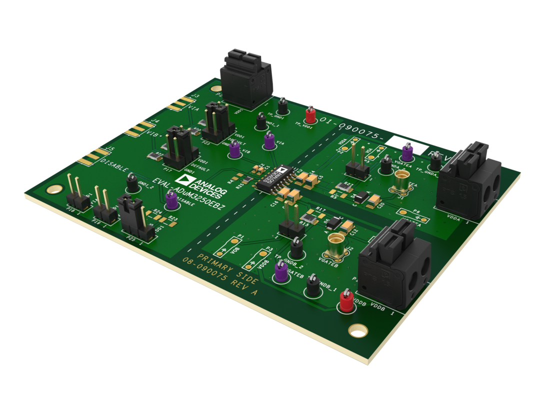
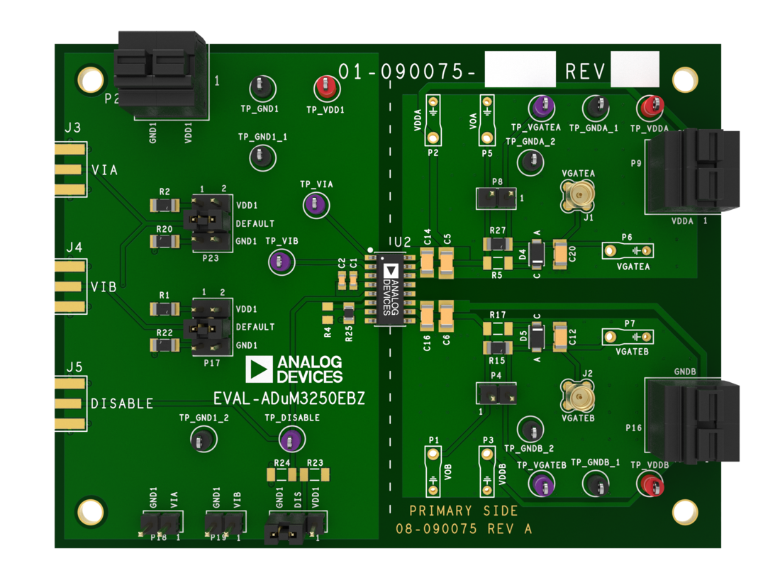
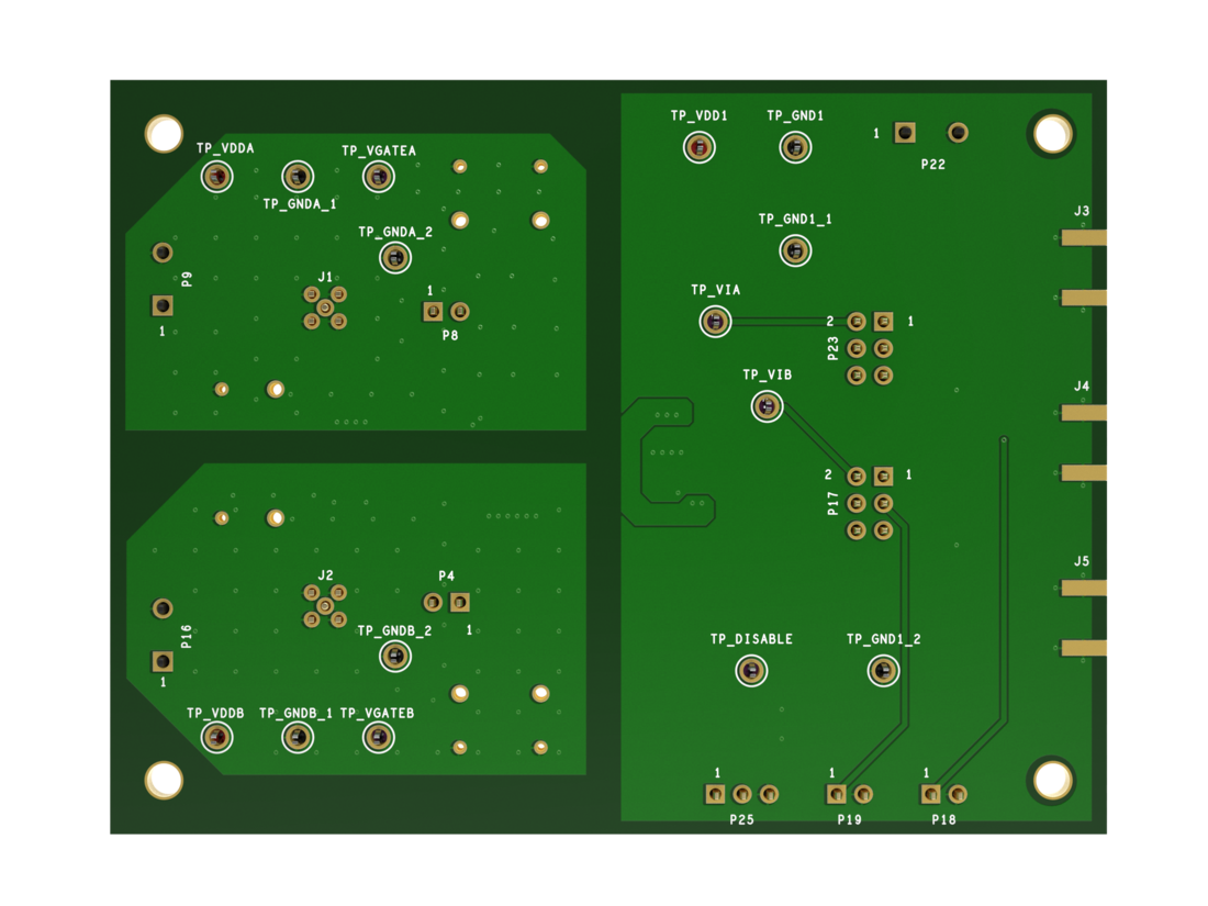
Evaluating the ADuM3250, Isolated, Half-Bridge Gate Driver with Adjustable Dead Time, 10A Output
资料
最新评论
需要发起讨论吗? 没有关于 ADUM3250的相关讨论?是否需要发起讨论?
在EngineerZone®上发起讨论