概要
設計リソース
設計/統合ファイル
• Schematic• Bill of Materials
• Assembly Drawing
• PADs Layout Files
• Gerber Files 設計ファイルのダウンロード 6.65 M
評価用ボード
型番に"Z"が付いているものは、RoHS対応製品です。 本回路の評価には以下の評価用ボードが必要です。
- EVAL-CN0359-EBZ ($162.43) Fully Automatic High Performance Conductivity Measurement System
機能と利点
- Conductivity Range of 0.1 μS to 10 S
- Automatic Measurement Ranging
- 2- or 4-wire Conductivity Probe Compatible
- External Temperature Compensation
- Standalone Operation and Control
参考資料
-
EVAL-CN0359-EBZ User Guide (GitHub)2026/04/16
-
CN-0359: 全自動の高性能かつ高効率な測定システム (Rev. 0)2023/03/28PDF261 K
-
自動校正機能を備える 導電率測定システム2016/11/01 アナログ・ダイアログ
回路機能とその特長
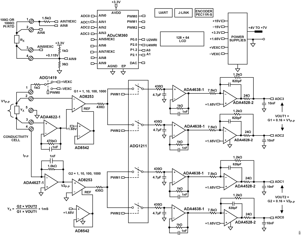
The circuit shown in Figure 1 is a completely self-contained, microprocessor controlled, highly accurate conductivity measurement system ideal for measuring the ionic content of liquids, water quality analysis, industrial quality control, and chemical analysis.
A high performance combination of precision signal conditioning components yields an accuracy of better than 0.3% over a conductivity range of 0.1 μS to 10 S (10 M to 0.1 Ω) with no calibration requirements, using either 2- or 4-wire conductivity cells.
The circuit automatically detects either 100 Ω or 1000 Ω platinum (Pt) resistance temperature devices in 2-, 3-, or 4-wire configurations, allowing for added flexibility when measuring the temperature of the liquid.
The circuit generates a precise AC excitation voltage with minimum dc offset to avoid a damaging polarization voltage on the conductivity electrodes. The amplitude and frequency of the AC excitation is user-programmable.
A synchronous sampling technique converts the peak-to-peak amplitude of the excitation voltage and current to a DC value for accuracy and ease in processing using the dual, 24-bit Σ-Δ ADC integrated within the precision analog microcontroller.
The user interface consists of an LCD display and an encoder push button. The circuit can also communicate with a PC using a USB-to-UART bridge if desired, and operates on a single 4 V to 7 V power supply.
回路説明
CONDUCTIVITY THEORY
The resistivity of a material or liquid is defined as the resistance of a cube of the material with perfectly conductive contacts on opposite faces. The resistance can be calculated using Equation 1:

where:
R is the resistance.
ρ is the resistivity of the material.
L is the distance between the contacts.
A is the area of the contacts.
Resistivity is measured in units of Ω cm. A 1 Ω cm material has a resistance of 1 Ω when contacted on opposite faces of a 1 cm × 1 cm × 1 cm cube.
Conductance is the reciprocal of resistance, and conductivity is the reciprocal of resistivity. The unit of measurement of conductance is Siemens (S), and the unit of measurement of conductivity is S/cm, mS/cm, or μS/cm.
All aqueous solutions conduct electricity to some degree. Adding electrolytes such as salts, acids, or bases to pure water increases the conductivity (and decreases resistivity).
For the purposes of this circuit note, Y is the general symbol for conductivity measured in S/cm, mS/cm, or μS/cm. However, in many cases, the distance term is dropped for convenience, and the conductivity is simply expressed as S, mS, or μS.
A conductivity system measures conductivity by means of electronics connected to a sensor called a conductivity cell immersed in a solution, as shown in Figure 2.

The electronic circuitry applies an alternating voltage on the sensor and measures the resulting current, which is related to the conductivity. Because conductivity has a large temperature coefficient (up to 4%/°C), a temperature sensor is incorporated into the circuitry to adjust the reading to a standard temperature, usually 25°C (77°F). When measuring solutions, the temperature coefficient of the conductivity of the water itself must be considered.
A basic conductivity sensor typically consists of two electrodes that are insulated from one another. The electrodes, typically Type 316 stainless steel, titanium palladium alloy, or graphite, are specifically sized and spaced to provide a known cell constant. Theoretically, a cell constant of 1.0/cm describes two electrodes, each sized 1 cm2 in area, and spaced 1 cm apart. Cell constants must be matched to the measurement system for a given range of operation.
For instance, if a sensor with a cell constant of 1.0/cm is used in pure water with a conductivity of 1 μS/cm, the cell has a resistance of 1 MΩ. Conversely, the same cell in seawater has a resistance of 30 Ω. Because the resistance ratio is so large, it is difficult for ordinary instruments to accurately measure such extremes with only one cell constant.
When measuring the 1 μS/cm solution, the cell is configured with large area electrodes spaced a small distance apart. For example, a cell with a cell constant of 0.01/cm results in a measured cell resistance of approximately 10,000 Ω rather than 1 MΩ. It is easier to accurately measure 10,000 Ω than 1 MΩ; therefore, the measuring instrument can operate over the same range of cell resistance for both ultrapure water and high conductivity seawater by using cells with different cell constants.
The cell constant is defined as the ratio of the distance between the electrodes to the area of the electrodes, which can be calculated using Equation 2:

where:
K is the cell constant in cm-1.
L is the distance between electrodes in cm.
A is the area of electrode surface in cm2.
The instrumentation then measures the cell conductance using Equation 3:

Y is the measured cell conductance in S.
I is the cell current.
V is the excitation voltage.
The conductivity of the liquid is then calculated using Equation 4:

Yx is the conductivity of the liquid in S/cm.
K is the cell constant in cm-1.
Y is measured conductance in S.
There are two types of conductivity cells: those with two electrodes, and those with four electrodes, as shown in Figure 3. The electrodes are often referred to as poles.
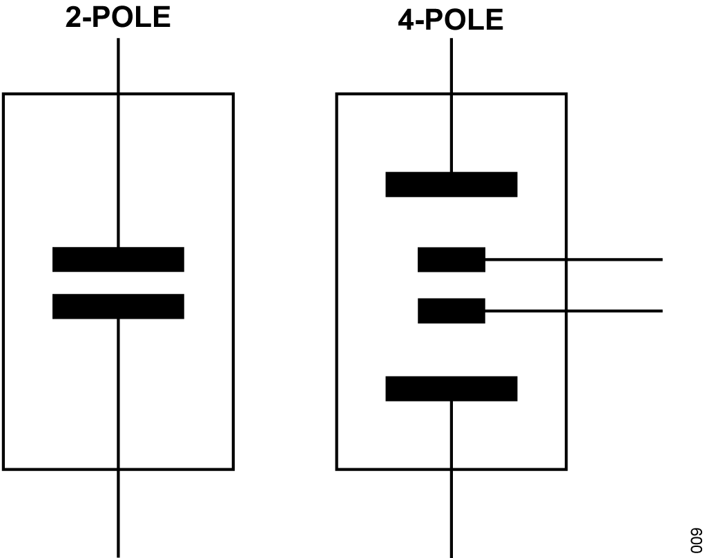
The 2-pole sensor is more suitable for low conductivity measurements, such as purified water, and various biological and pharmaceutical liquids. The 4-pole sensor is more suitable for high conductivity measurements, such as waste water and seawater analysis.
The cell constants for 2-pole cells typically range from approximately 0.1/cm to 1/cm, and the cell constants for 4-pole cells typically range from 1/cm to 10/cm.
The 4-pole cell eliminates the errors introduced by polarization of the electrodes and field effects that can interfere with the measurement.
The actual configuration of the electrodes can be that of parallel rings, coaxial conductors, or others, rather than the simple parallel plates shown in Figure 2.
Regardless of the type of cell, it is important not to apply a DC voltage to any electrode, because ions in the liquid accumulate on the electrode surface, thereby causing polarization, measurement errors, and damage to the electrode.
Take special care with sensors that have shields, as in the case of coaxial sensors. Connect the shield to the same potential as the metal container holding the liquid. If the container is grounded, connect the shield to the circuit board ground.
The final precaution is not to exceed the rated excitation voltage or current for the cell. The CN0359 circuit allows programmable excitation voltages from 100 mV to 10 V, and the 1 kΩ series resistor limits the maximum cell current to 10 mA.
EXCITATION GENERATION
The excitation square wave for the conductivity cell is generated by switching the ADG1419 between the +VEXC and −VEXC voltages using the pulse-width modulation (PWM) output of the ADuCM360 microcontroller. It is important that the square wave has a precise 50% duty cycle and a very low DC offset. Even small DC offsets can damage the cell over a period of time.
The +VEXC and −VEXC voltages are generated by the ADA4077-2 op amps, and their amplitudes are controlled by the DAC output of the ADuCM360, as shown in Figure 4.
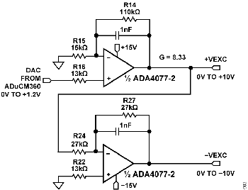
The ADA4077-2 has a typical offset voltage of 15 μV (A grade), a 0.4 nA bias current, and a 0.1 nA offset current, which minimizes residual DC content of the excitation waveform. Output current is up to ±10 mA, allowing use with very high conductivity liquids; and the low 1.2 V dropout maximizes the available output swing.
The ADA4077-2 op amp has a closed-loop gain of 8.33 and converts the ADuCM360 internal DAC output (0 V to 1.2 V) to the +VEXC voltage of 0 V to 10 V. The second ADA4077-2 op amp inverts the +VEXC and generates the −VEXC voltage. R22 is chosen such that R22 = R24||R27 to achieve first-order bias current cancellation. The error due to the 15 μV offset voltage of the first ADA4077-2 op amp is approximately (2 × 15 μV) ÷ 10 V = 3 ppm. The primary error introduced by the inverting stage is therefore the error in the resistor matching between R24 and R27.
The ADG1419 is a 2.1 Ω, on-resistance SPDT analog switch with an on-resistance flatness of 50 mΩ over a ±10 V range, making it ideal for generating a symmetrical square wave from the ±VEXC voltages. The ADG1419 introduces a symmetrical error of 50 mΩ ÷ 1 kΩ = 50 ppm (Typical).
ANALOG SIGNAL CONDITIONING
The voltage applied to the conductivity cell is measured with the AD8253 instrumentation amplifier. The positive input to the AD8253 is buffered by the ADA4622-1. The ADA4622-1 is chosen based primarily on its bias current of 5 pA to minimize the error in measuring low currents associated with low conductivities. The negative input of the AD8253 does not require buffering.
The offset voltages of AD8253 and ADA4638-1 are removed by the synchronous sampling stage and do not affect the measurement accuracy.
The AD8253 instrumentation amplifiers have a high bandwidth of 10 MHz, programmable gains of 1, 10, 100, 1000, and a gain error of less than 0.04%. The AD8253 also has a slew rate of 20 V/μs and a settling time of 1.8 μs to 0.001% for G = 1000. The fixed, selectable gains provide a wide measurement range, and the fast slew rate ensures that the output is fully settled before sampling.
The ADA4627-1 stage is a precision current to voltage converter that converts the current through the sensor to a voltage. The low bias current and offset voltage of the ADA4627-1 has typical values of 1 pA and 120 μV, respectively (A grade); making it an ideal component selection for this stage of the design. The symmetrical error produced by the 120 μV offset error is only 120 μV/10 V = 12 ppm.
ADC CAPTURE AND MEASUREMENT
The ADuCM360 generates the PWM0 square wave switching signal for the ADG1419 switch, as well as PWM1 and PWM2 synchronizing signals for the synchronous sampling stages. The cell voltage and the three timing waveforms are shown in Figure 5.

The output of the AD8253 in amp drives two parallel track-and-hold circuits composed of ADG1211 switches, series resistors, hold capacitors, and unity-gain buffers.
The ADG1211 is a low charge injection, quad SPST analog switch, operating on a ±15 V power supply with up to ±10 V input signals. The maximum charge injection due to switching is 4 pC, which produces a voltage error of only 4 pC ÷ 4.7 μF = 0.9 μV.
The PWM1 signal causes the ADA4638-1 track-and-hold buffer to track the negative cycle of the sensor voltage and then hold it until the next track cycle. The output of the ADA4638-1 track-and-hold buffer is therefore a DC level corresponding to the negative amplitude of the sensor voltage square wave.
Similarly, the PWM2 signal causes the other ADA4638-1 track-and-hold buffer to track the positive cycle of the sensor voltage and then hold it until the next track cycle. The output of the other ADA4638-1 track-and-hold buffer is therefore a DC level corresponding to the positive amplitude of the sensor voltage square wave.
The bias current of the ADA4638-1 track-and-hold buffers is 45 pA typical, and the leakage current of the ADG1211 switch is 20 pA typical. Therefore, the worst-case leakage current on the 4.7 μF hold capacitors is 65 pA. For a 100 Hz excitation frequency, the period is 10 ms. The drop voltage over one-half the period (5 ms) due to the 65 pA leakage current is (65 pA × 5 ms) ÷ 4.7 μF = 0.07 μV.
The offset voltage of the ADA4638-1 zero-drift amplifier is only 0.5 μV typical and contributes negligible error.
The final stages in the signal chain before the ADC are the ADA4528-2 inverting attenuators that have a gain of −0.16 and a common-mode output voltage of +1.65 V. The ADA4528-2 has an offset voltage of 0.3 μV typical and therefore contributes negligible error.
The attenuator stage reduces the ±10 V maximum signal to ±1.6 V with a common-mode voltage of +1.65 V. This range is compatible with the input range of the ADuCM360 ADC input, which is 0 V to 3.3 V (1.65 V ± 1.65 V) for an AVDD supply of 3.3 V.
CALCULATING CONDUCTIVITY
The four output voltages of the analog front end signal chain represent the sampled current and voltage values of the conductivity cell during the positive and negative halves of the excitation cycle. The two outputs of the cell voltage measurement circuit are applied to the AIN2 and AIN3 pins of the ADuCM360. Similarly, the two outputs of the cell current measurement circuit are applied to the AIN0 and AIN1 pins.
To obtain peak-to-peak values from these outputs, the internal ADC of the ADuCM360 is configured for differential mode. As such, the four individual outputs of the analog front end are reduced to two differential voltages that will be read by the ADuCM360. The two differential output voltages are given by Equation 5 and Equation 6:


where:
VOUT1 is the differential ADC voltage representing the peak-to-peak cell voltage in V.
VOUT2 is the differential ADC voltage representing the peak-to-peak cell current in V.
ADC0 is the AIN0 input voltage in V.
ADC1 is the AIN1 input voltage in V.
ADC2 is the AIN2 input voltage in V.
ADC3 is the AIN3 input voltage in V.
These differential voltages are used by the ADuCM360 to determine the cell conductance and the conductivity of the liquid under test. As shown in Equation 7, the cell conductance is equal to the peak-to-peak cell current divided by the peak-to-peak cell voltage:

where:
Y is the cell conductance in S.
IP-P is the peak-to-peak cell current in A.
V1P-P is the peak-to-peak cell voltage in V.
Since the cell current is converted into a voltage signal by the feedback resistor of the ADA4627-1, its peak-to-peak value can be derived using Equation 8:

where:
V2P-P is the peak-to-peak output of the ADA4627-1 in V.
Rf is the ADA4627-1 feedback resistance in Ω.
The peak-to-peak cell voltage can be derived from the differential outputs of the analog front end, as shown in Equation 9 and Equation 10:


where:
G1 is the AD8253 gain setting in the cell voltage measurement circuit.
G2 is the AD8253 gain setting in the cell current measurement circuit.
α is the attenuation from the ADA4528-2 stage.
By combining Equation 8 and Equation 10, an expression can be obtained for IP-P:

Finally, by substituting Equation 9 and Equation 11 back into Equation 7, the general formula for conductance as a factor of the differential ADC measurements can be written as:

In this reference design, the ADA4627-1 feedback resistor has a value of 1 kΩ resulting in Equation 13:

From the cell conductance, the ADuCM360 can then calculate the conductivity of the liquid based on the cell constant of the sensor as shown in Equation 14:

where:
Yx is the conductivity of the liquid under test in S/cm.
Y is the measured cell conductance.
K is the cell constant in cm-1.
SYSTEM ACCURACY MEASUREMENTS
Equation 9 through Equation 13 are all based on the assumption that the four individual ADA4528-2 op amps provide the same attenuation value of 0.16; any deviation would introduce an error in the final measurements. Since the attenuation of an ADA4528-2 op amp is dependent on its feedback resistance and input resistance, the resistors used for these should be matched as closely as possible with their counterparts in each channel to maintain the system accuracy.
Equation 13 also shows that the conductivity measurement depends on G1, G2, and Rf, and the ratio of VOUT2 to VOUT1. Therefore, a precision reference is not required for the ADCs within the ADuCM360.
Additionally, the conductance calculation performed by the ADuCM360 assumes an exact 1 kΩ value for the ADA4627-1 feedback resistance, as shown in Equation 13. The farther the actual resistance is from this ideal value, the greater the error introduced into the calculation; therefore, it is imperative that a high precision resistor be used for the ADA4627-1 feedback.
Assuming that all nine resistors have 0.1% tolerance, and including the 0.04% (max) gain error of the AD8253, a worst-case error analysis yields approximately 0.6%.
In practice, the resistors are more likely to combine in an RSS manner, and the RSS error due to the resistor tolerances in the positive or negative signal chain is √5 × 0.1% = 0.22%.
Accuracy measurements were taken using precision resistors from 1 Ω to 1 MΩ (1 S to 1 μS) to simulate the conductivity cell. Figure 6 shows the results, and the maximum error is less than 0.1%.
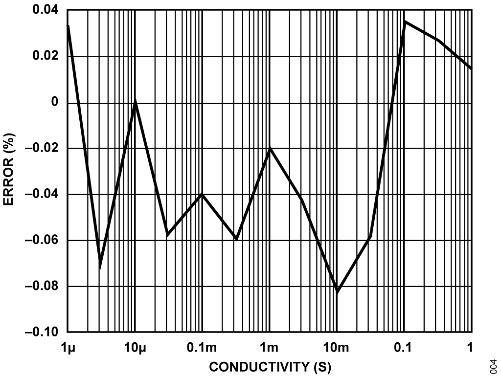
In order to maintain accuracy over a wide input range with a high signal-to-noise ratio, a given measurement must use a large fraction of the ADC's input range without exceeding full-scale. The CN0359's software implements a simple autoranging scheme, adjusting the AD8253's gain to maintain the ADC's input between 10% and 90% of full-scale.
PREVENTING ELECTROLYSIS AND POLARIZATION
For proper conductivity measurements, it is critical to prevent electrolysis of the sample solution and polarization of the cell electrodes. Electrolysis is a chemical reaction caused by applying an excessively large voltage level to the conductivity cell, and changes the conductivity of the sample solution over time. Polarization of the conductivity cell occurs when current is allowed to flow across the electrodes in one direction for a sufficiently long time. In this scenario, ions accumulate on the surfaces of the electrodes, resulting in the formation of a space charge region, and thereby restricting the flow of current. Both electrolysis and polarization introduce nonlinear errors to the measurements, and therefore result in erroneous readings.
To avoid these errors, the level and frequency of the excitation signal should be set appropriately based on the specifications of the conductivity cell. In addition, the DC content of this waveform should be kept to a minimum to prevent DC currents from appearing across the cell electrodes.
The CN0359 is carefully designed for low DC voltage bias on the excitation channel, with typical values being less than 200 μV. For most commercial conductivity probes, this small residual DC content has negligible effect. Certain probes however, depending on their construction, can be more sensitive and might exhibit a drift in measurement values. For these cases, capacitive coupling should be used for the voltage measurement channel.
RTD MEASUREMENT
Conductivity measuring system accuracy is only as good as its temperature compensation. Because common solution temperature coefficients vary in the order of 1%/°C to 3%/°C or more, the CN0359 implements a temperature compensation scheme. Solution temperature coefficients are somewhat nonlinear and usually vary with the actual conductivity as well. Therefore, calibration at the actual measuring temperature yields the best accuracy.
The ADuCM360 contains two matched, software configurable, excitation current sources. They are individually configurable to provide a current output of 10 μA to 1 mA, and matching is better than 0.5%. The current sources allow the ADuCM360 to easily perform 2-wire, 3-wire, or 4-wire measurements for either Pt100 or Pt1000 RTDs. The software also automatically detects if the RTD is Pt100 or Pt1000 during the set up procedure.
The following discussion shows simplified schematics of how the different RTD configurations operate. All mode switching is accomplished in the software, and there is no need to change the external jumper settings.
Figure 7 shows the configuration for 4-wire RTDs.

The parasitic resistance in each of the leads to the remote RTD is shown as RP. The excitation current passes through a precision 1.5 kΩ resistor and the RTD. The on-chip ADC measures the voltage across the resistor.
It is important that the 1.5 kΩ resistor (REXC) and the excitation current (IEXC) value be chosen such that the ADuCM360 maximum input voltage at AIN7 does not exceed AVDD − 1.1 V; otherwise, the IEXC current source does not function properly.
The RTD voltage is accurately measured using the two sense leads that connect to AIN6 and AIN5. The input impedance is approximately 2 MΩ (unbuffered mode, PGA gain = 1), and the current flowing through the sense lead resistance produces minimum error. The ADC then measures the RTD voltage.
The RTD resistance is then calculated using Equation 15:

where:
Rx is the RTD resistance value.
ADC5 is the AIN5 input voltage in V.
ADC6 is the AIN6 input voltage in V.
ADC7 is the AIN7 input voltage in V.
ADC8 is the AIN8 input voltage in V.
The measurement is ratiometric and does not depend on an accurate external reference voltage, only the tolerance of the 1.5 kΩ resistor. In addition, the 4-wire configuration eliminates the error associated with the lead resistances.
The ADuCM360 has a buffered or unbuffered input option. If the internal buffer is activated, the input voltage must be greater than 100 mV. The 1 kΩ/36 Ω resistor divider provides a 115 mV bias voltage to the RTD that allows buffered operation. In the unbuffered mode, Terminal 4 of J3 can be grounded and connected to a grounded shield for noise reduction.
The 3-wire connection is another popular RTD configuration that eliminates lead resistance errors, as shown in Figure 8.
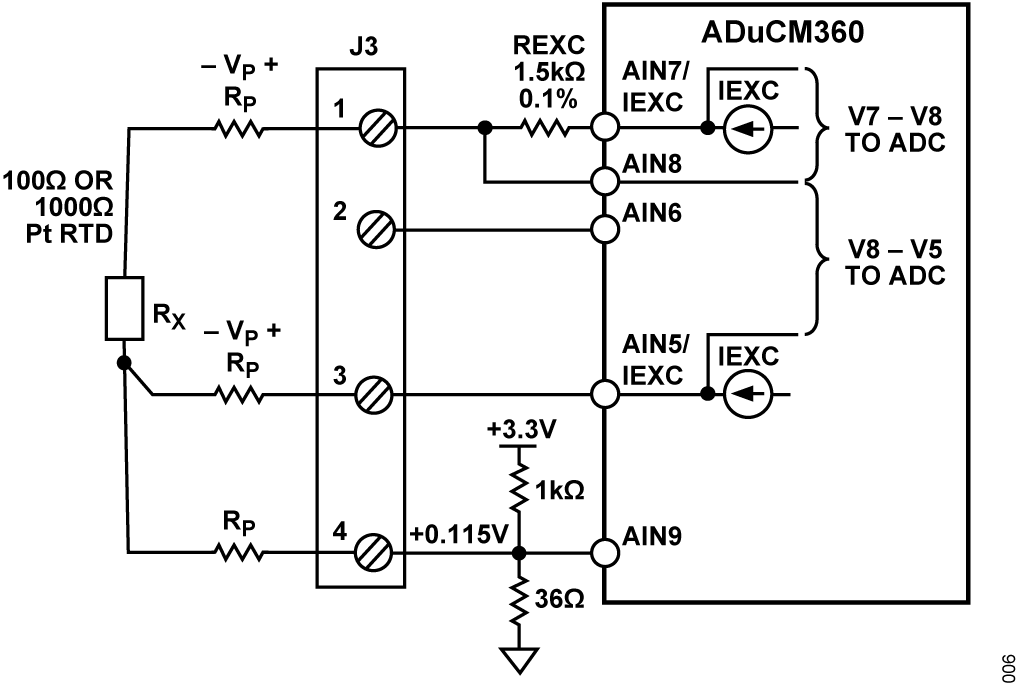
The second matched IEXC current source (AIN5/IEXC) develops a voltage across the lead resistance in series with Terminal 3 that cancels the voltage dropped across the lead resistance in series with Terminal 1. The measured voltage is therefore free of lead resistance error. The RTD resistance can be calculated using Equation 16:

where:
Rx is the RTD resistance value.
ADC5 is the AIN5 input voltage in V.
ADC7 is the AIN7 input voltage in V.
ADC8 is the AIN8 input voltage in V.
Figure 9 shows the 2-wire RTD configuration where there is no compensation for lead resistance. The RTD resistance for 2-wire configuration can be calculated as Equation 17:

where:
Rx is the RTD resistance value.
ADC7 is the AIN7 input voltage in V.
ADC8 is the AIN8 input voltage in V.
ADC9 is the AIN9 input voltage in V.
RP is the parasitic resistance value.
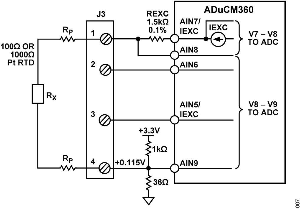
The 2-wire configuration is the lowest cost circuit and is suitable for less critical applications, short RTD connections, and higher resistance RTDs such as Pt1000.
POWER SUPPLY CIRCUITRY
To simplify system requirements, all the required voltages (±15 V and +3.3 V) are generated from a single 4 V to 7 V supply, as shown in Figure 10.
The ADP2300 buck regulator generates the 3.3 V supply for the board. The design is based on the downloadable ADP230x Buck Regulator Design Tool.
The ADP5072 switching regulator generates independently regulated +15 V and -15 V supply rails for the different amplifiers. This design follows the typical application circuit shown in the ADP5072 data sheet, and uses the recommended component values for a +3.3 V to ±15 V application.
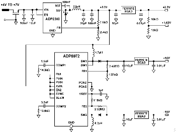
Figure 11 shows the LCD backlight driver circuit. The AD8592 op amp acts as a 30 mA current source to supply the LCD backlight current. The AD8592 can source and sink up to 250 mA, and the 100 nF capacitor ensures a soft startup.

バリエーション回路
The system shown in the CN0359 uses the ADuCM360 precision analog microcontroller for a highly integrated conductivity measurement. If the user desires a discrete ADC, the AD7794 24-bit, Σ-Δ ADC is a good choice.
If board space is at a premium, the ADP2300 buck regulator can be replaced with a μModule® part such as the LTM8074. While a more expensive solution compared to the ADP2300, the LTM8074 is a highly integrated device with the inductor already built into its package and does not require a catch diode. It is also designed with the low noise Silent Switcher® architecture, which allows for minimal electromagnetic interference (EMI) during operation.
Certain conductivity measurement applications may have additional requirements such as isolation or a small hardware footprint. As such, Analog Devices, Inc. also offers other reference designs with varying form-factors and features. One of these is the CN0349, which features a high precision conductivity measurement data acquisition system with an 8-pin I2C Pmod interface that is ideal for industrial environments that require a small, low cost, fully isolated solution. Other examples are the CN0411 and the CN0428, which are designed to measure conductivity for water quality monitoring applications.
回路の評価とテスト
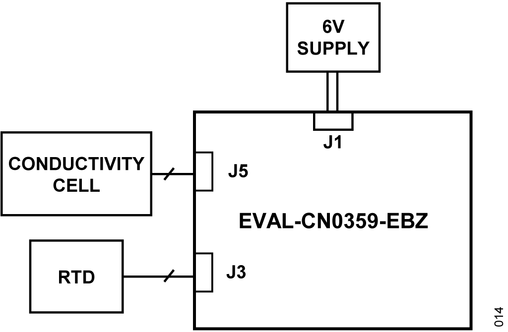
This circuit uses the EVAL-CN0359-EBZ circuit board, an external power supply, conductivity cell, and an RTD. The EVAL-CN0359-EBZ comes preloaded with the code required to make the conductivity measurements. For complete information on the system hardware and software operation, refer to the CN0359 User Guide.
EQUIPMENT NEEDED
The following equipment is needed:
- The EVAL-CN0359-EBZ circuit board
- A 6 V power supply or wall wart (EVAL-CFTL-6V-PWRZ)
- A conductivity cell
- Pt100 or Pt1000 2-wire, 3-wire, or 4-wire RTD (if the RTD is not connected, the conductivity measurement is referenced to 25°C)
SETUP
Use the following steps to setup the CN0359 for evaluation:
- Connect the 6 V power supply (EVAL-CFTL-6V-PWRZ) to the EVAL-CN0359-EBZ.
- Enter parameters for EXC Voltage, EXC Frequency, TEMP Coefficient, and Cell Constant that are appropriate for the probe.
- Disconnect the EVAL-CFTL-6V-PWRZ power supply.
- Connect the conductivity cell as follows:
- 4-wire cell: connect an outside current electrode to J5 Pin 1 and the closest inner voltage electrode to J5 Pin 2. Connect the second outside current electrode to J5 Pin 4 and the closest inner voltage electrode to Pin 3.
- 2-wire cell: connect one electrode to J5 Pin 1 and Pin 2 and connect the second electrode to J5 Pin 2 and Pin 4.
- If the conductivity cell has a shield, connect it to J5 Pin 5.
- Connect the RTD as follows (if used):
- 4-wire RTD (see Figure 7): Pair up the four wires according to their color (or other identifying characteristic). Connect one pair of wires to J3 Pin 1 and Pin 2, and the other pair to J3 Pin 3 and Pin 4. Only one wire should be connected to each pin.
- 3-wire RTD (see Figure 8: Connect the odd wire to J3 Pin 1, and the two common wires to J3 Pin 3 and Pin 4. Only one wire should be connected to each pin.
- 2-wire RTD (see Figure 9): connect one RTD wire to J3 Pin 1 and the other wire to J3 Pin 4.
- If the RTD wires are shielded, connect the shield to J5 Pin 5.
- Reconnect the EVAL-CFTL-6V-PWRZ power supply to the EVAL-CN0359-EBZ.
- Wait for the ADuCM360 to flush the buffers and display the conductivity and the temperature. If the screen shows an error and the buzzer beeps more than 20 times, check the sensor connections.
Figure 12 shows a typical conductivity measurement setup.
