概要
設計リソース
設計/統合ファイル
• Schematic• Bill of Materials
• Gerber Files
• Layout Files (Altium)
• Assembly Drawing 設計ファイルのダウンロード 2.46 M
評価用ボード
型番に"Z"が付いているものは、RoHS対応製品です。 本回路の評価には以下の評価用ボードが必要です。
- EVAL-CN0349-PMDZ ($60.92) Fully Isolated Conductivity Measurement Data Acquisition System
- EVAL-SDP-CB1Z ($134.00) Eval Control Board
- SDP-PMD-IB1Z ($74.45) PMOD to SDP Interposer Board
デバイス・ドライバ
コンポーネントのデジタル・インターフェースとを介して通信するために使用されるCコードやFPGAコードなどのソフトウェアです。
機能と利点
- Accurate conductivity measurements to 1%
- Small PCB footprint
- Fully isolated
参考資料
-
CN0349 Software User Guide2018/10/16WIKI
-
CN0349: Fully Isolated Conductivity Measurement Data Acquisition System (Rev. A)2017/06/12PDF413 K
回路機能とその特長
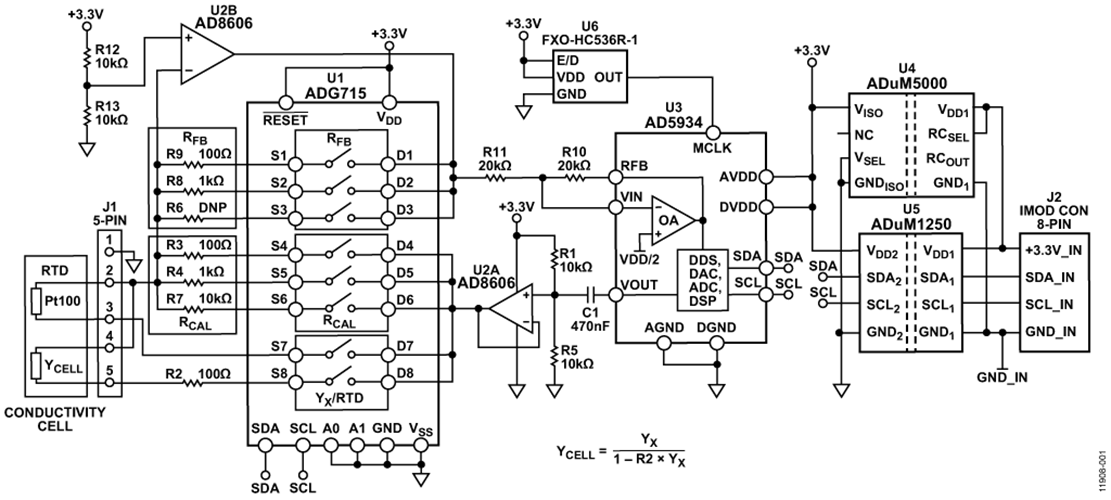
The circuit shown in Figure 1 provides a complete, robust data acquisition solution for processing conductivity cell outputs, including temperature correction. This circuit is ideal for measuring the ionic content of liquids, water quality analysis, and chemical analysis.
This design solution is optimized for high precision and low cost, and it uses only five active devices. The circuit has a total error of less than 1% FSR after calibration. The small footprints of all the components make the circuit ideal for applications where printed circuit board (PCB) real estate is a premium. The digital output of the circuit is fully isolated; therefore, the ground loop interference is eliminated, making it ideal for harsh industrial environments.

回路説明
The circuit shown in Figure 1 incorporates the AD5934 12-bit impedance converter, the ADG715 octal single-pole, single-throw (SPST) switch, the AD8606 rail-to-rail op amp, the ADuM1250 dual I2C isolator, and the ADuM5000 isolated dc-to-dc converter to create a complete data acquisition system for conductivity measurements. The circuit has an 8-pin IMOD connector on board that can be used for connection to a customer microprocessor or a field programmable gate array (FPGA).
The AD5934 is a high precision impedance converter system solution that combines an on-chip, programmable direct digital synthesizer (DDS) with a 12-bit, 250 kSPS analog-to-digital converter (ADC). The tunable frequency generator allows an external complex impedance to be excited with a known frequency. The AD5933 is a similar device with a 1 MSPS ADC. The on-board ADC monitors the voltage and current of the unknown impedance. An on-board digital signal processor (DSP) engine calculates the discrete Fourier transform (DFT). The DFT algorithm returns a real (R) and an imaginary (I) data-word at each output frequency.
The AD8606 op amp was chosen because of its low offset voltage (65 μV maximum), low bias current (1 pA maximum), and low noise (12 nV/√Hz maximum).
The ADG715 is a complementary metal oxide semiconductor (CMOS), octal SPST switch that is controlled via a 2-wire serial interface that is compatible with the I2C interface standard. Low power consumption, a low operating supply range of 2.7 V to 5.5 V, low on-resistance (typically 2.5 Ω), and a small 24-lead TSSOP package make this device ideal for many applications.
The ADuM5000 is an isolated dc-to-dc converter with a 3.3 V or 5 V output, based on the Analog Devices isoPower® technology, and packaged in a 16-lead SOIC.
The ADuM1250 is a hot swappable, digital isolator with non-latching, bidirectional communication channels that are compatible with I2C interfaces, based on the iCoupler chip scale transformer technology from Analog Devices, Inc., and packaged in an 8-lead SOIC.
Conductivity Theory
The resistivity, ρ, of a material or liquid is defined as the resistance of a cube of the material with perfectly conductive contacts on opposite faces. The resistance for other shapes can be calculated by
R = ρL/A
where:
L is the distance between the contacts.
A is the area of the contacts
Resistivity is measured in units of Ω cm. A 1 Ω cm material has a resistance of 1 Ω when contacted on opposite faces of a 1 cm × 1 cm × 1 cm cube.
Conductance is the reciprocal of resistance, and conductivity is the reciprocal of resistivity.
All aqueous solutions conduct electricity to some degree. The measure of the ability of a solution to conduct electricity is called conductance, and it is the reciprocal of resistance. The unit of measurement of conductance is Siemens (S). Adding electrolytes such as salts, acids, or bases to pure water increases the conductance (and decreases resistance). Resistivity is expressed in Ω cm, and conductivity is expressed in S/cm, mS/cm, or μS/cm.
For the purposes of this circuit note, Y is used as the general symbol for conductivity measured in S/cm, mS/cm, or μS/cm. However, in many cases, the distance term is dropped for convenience, and the conductivity is simply expressed as S, mS, or μS.
A conductivity system measures conductance by means of electronics connected to a sensor immersed in a solution. The analyzer circuitry impresses an alternating voltage on the sensor and measures the size of the resulting current, which is related to the conductivity. Because conductivity has a large temperature coefficient (up to 4%/°C), an integral temperature sensor is incorporated into the circuitry to adjust the reading to a standard temperature, usually 25°C (77°F). When measuring solutions, the temperature coefficient of the conductivity of the water itself must be considered. To compensate accurately for the temperature, a second temperature sensor and compensation network must be used.
Conductivity Sensors
The contacting type sensor usually consists of two electrodes that are insulated from one another. The electrodes, typically Type 316 stainless steel, titanium palladium alloy, or graphite, are specifically sized and spaced to provide a known cell constant. Theoretically, a cell constant of 1.0/cm describes two electrodes, each sized one square centimeter in area, and spaced one centimeter apart. Cell constants must be matched to the analyzer for a given range of operation. For instance, if a sensor with a cell constant of 1.0/cm is used in pure water with a conductivity of 1 μS/cm, the cell has a resistance of 1 MΩ. Conversely, the same cell in seawater has a resistance of 30 Ω. Because the resistance ratio is so large, it is difficult for ordinary instruments to accurately measure such extremes with only one cell constant.
When measuring the 1 μS/cm solution, the cell is configured with large electrodes spaced a small distance apart. For example, a cell with a cell constant of 0.01/cm results in a cell resistance of approximately 10,000 Ω, which can be measured quite accurately. Therefore, the measuring instrument can operate over the same range of cell resistance for both ultra-pure water and high conductivity seawater, by using cells with different cell constants.
Temperature Compensation
Conductivity measuring system accuracy is only as good as its temperature compensation. Because common solution temperature coefficients vary in the order of 1%/°C to 3%/°C, or more, measuring instruments with adjustable temperature compensation must be used. Solution temperature coefficients are somewhat nonlinear and usually vary with the actual conductivity as well. Thus, calibration at the actual measuring temperature yields the best accuracy.
The circuit shown in Figure 1 yields accurate conductivity measurements, extending from the low μS range to several hundred mS, and it also optimizes the overall accuracy of the AD5934 over a wide range of admittance. Temperature measurement using a Pt100 resistance temperature detector (RTD) is also incorporated. The circuit can be connected to the evaluation microprocessor board using the 8-pin IMOD (I2C interface) connector for rapid prototyping (Digilent, Pmod™ Specifications).
The circuit consists of four major blocks. The first block is an impedance-to-digital converter containing the AD5934 (U3) impedance converter, a follower (one half of the AD8606, U2A) to bias the ac signal to VDD/2, and a current-to-voltage converter configuration using the second half of the AD8606, U2B. Details of the operation of the AD5934 can be found in Circuit Note CN-0217 and in the AD5934 data sheet.
The second block is the programmable resistor feedback (R6, R8, R9) and calibration (R3, R4, R7) circuitry and the octal SPST switches ADG715 (U1). The measurement range and calibration procedures are realized by controlling the ADG715 via the I2C serial interface.
The third and fourth blocks are optional; however, they provide galvanic isolation between the circuit and the evaluation micro-processor board. They are not required unless isolation is needed.
The circuit is connected to the conductivity cell with a built-in Pt100 RTD temperature sensor using the CON1 (J1) connector.
The frequency of the clock applied to the MCLK pin is set to 1 MHz using a stable, low jitter, FXO-HC536R-1 (U6) quartz crystal oscillator. This oscillator allows the AD5934 to excite the conductivity cell with a frequency of 2 kHz, which is well suited for conductivity measurements.
Circuit Design
Figure 2 shows the optimized signal chain for conductivity and temperature measurements used in the circuit. The AD5934 has four programmable output voltage ranges. Each range has an associated output impedance. For example, the output impedance for a 1.98 V p-p output voltage is typically 200 Ω (see the AD5934 data sheet). The output impedance affects the impedance measurement accuracy, particularly in the low ohms range. A simple buffer in the signal chain prevents the output impedance from affecting the unknown impedance measurement. A low output impedance amplifier, with sufficient bandwidth to accommodate the AD5934 excitation frequency, is selected. An example of the low output impedance that can be achieved is shown in Figure 2 for the AD8605/AD8606/AD8608 family of CMOS op amps. The output impedance for this amplifier, for a gain of 1 is less than 1 Ω up to 100 kHz, which corresponds to the maximum operating range of the AD5934.
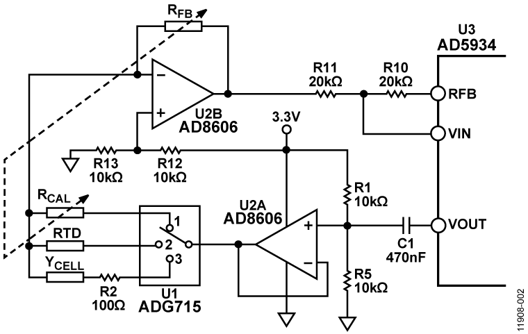
The four programmable output voltage ranges in the AD5934 have four associated bias voltages (see the AD5934 data sheet). For example, the 1.98 V p-p excitation voltage requires a bias of 1.48 V. However, the current-to-voltage (I-V) receiver stage of the AD5934 is set to a fixed bias of VDD/2. Therefore, for a 3.3 V supply, the transmit bias voltage is 1.48 V, and the receive bias voltage is 3.3 V/2 = 1.65 V. This potential difference polarizes the measured solution, YCELL, and can cause significant inaccuracies in the conductivity measurement. One solution is to add a simple high-pass filter with a corner frequency in the low Hz range (see the Circuit Note CN-0217). Removing the dc bias from the transmit stage and rebiasing the ac signal to VDD/2 keeps the dc level constant throughout the signal chain. Use precision 0.1% resistors for both of the biasing resistors, R1 and R5 (10 kΩ), to reduce inaccuracies. The I-V amplifier stage of the AD5934 can also add minor inaccuracies to the signal chain. The I-V conversion stage is sensitive to the amplifier bias current, to the offset voltage, and to the common-mode rejection (CMR). Accuracy is improved by selecting the proper external discrete amplifier (U2B) to perform the I-V conversion. The AD8606 is chosen because of its low offset voltage (65 μV maximum), low bias current (1 pA maximum), high CMRR (95 dB typically), and low noise (12 nV/√Hz maximum). The internal amplifier can then be configured as a simple inverting gain stage. Selection of the RFB resistor depends on the gain through the system, as described in the AN-1252 Application Note. The input and output of the I-V converter must be accurately biased to VDD/2. Use precision 0.1% resistors for both of the biasing resistors, R12 and R13 (10 kΩ). The accuracy is very much dependent on how large the unknown impedance range (conductivity range) is, relative to the calibration resistor, RCAL (see Circuit Note CN-0217 and Application Note AN-1252). Choosing an RCAL close to the unknown impedance achieves a more accurate measurement; that is, the closer the unknown impedance range is centered around RCAL, the more accurate the measurement. Consequently, for large unknown impedance ranges, it is possible to switch between various RCAL resistors, as is shown in Figure 2. Using various feedback resistor (RFB) values (see Figure 2) can optimize the dynamic range of the signal seen by the ADC. To improve the accuracy in the large range of conductance shown in Figure 1, three calibration resistors, RCAL (100 Ω, 1 kΩ, and 10 kΩ), and two feedback resistors, RFB (100 Ω and 10 kΩ), are used, controlled by the software and the ADG715 octal switches. The circuit is set to operate in two ranges:
- Low range: μS to mS, RFB = 1 kΩ, RCAL =1 kΩ and 10 kΩ
- High range: mS to S, RFB = 100 Ω, RCAL = 100 Ω and 1 kΩ
Using these two ranges, the total measuring range is 25 μS to 200 mS, with an accuracy higher than 1% FSR, as shown in the test data. Other values of RCAL and RFB can be chosen to cover different ranges.
Please note: If implementing the CN0349 software in MCU firmware, the settings in the ADG715 usage Table 1 should be followed.
| ADG715 Register Value | Allowable Settings |
| 0x09—High YX Range Calibration | Calibrate for RFB = R9 = 100 Ω, RCAL = R3 = 100 Ω |
| 0x11—High YX Range Calibration | Calibrate for RFB = R9 = 100 Ω, RCAL = R4 = 1 kΩ |
| 0x12—Low YX Range Calibration | Calibrate for RFB = R8 = 1 kΩ, RCAL = R4 = 1 kΩ |
| 0x22—Low YX Range Calibration | Calibrate for RFB = R8 = 1 kΩ, RCAL = R7 = 10 kΩ |
| 0x41—Measure RTD Value | Measure RTD with RFB = R9 = 100 Ω |
| 0x81—High YX Range Measurement | Measure YX with RFB = R9 = 100 Ω |
| 0x82—Low YX Range Measurement | Measure YX with RFB = R8 = 1 kΩ |
The CN0349 Evaluation Software allows the circuit to operate in three modes. In Mode 1 (Position 1 of the switch in Figure 2), the calibration procedure for both the low range and the high range is performed automatically. In Mode 2 (Position 2 of the switch in Figure 2), the temperature measurement of the solution is carried out automatically using an external Pt100 RTD temperature sensor. In Mode 3 (Position 3 of the switch in Figure 2), the actual conductivity of the solution is measured.
Calibration Procedure
For the circuit shown in Figure 1, the calibration procedure uses a three point calibration with three precision resistors, RCAL (R3 = 100 Ω, R4 = 1 kΩ, and R7 = 10 kΩ), minimizing offset and gain errors and linearizing the system within each range. For each range, the calibration procedure is performed at the beginning and at the end of the input range, by using two reference signals (calibration resistors), YL and YH, as is shown in Figure 3. The values of the reference signals are preloaded in the memory of the microcontroller or they can be input through the keyboard.
For the low range calibration point, the reference signal is YL (for example, YL = 1/R7 = 1/10 000 Ω = 0.1 mS). When the reference signal YL is connected, a code NL (Magnitude ML), corresponding to the reference signal YL, is obtained. Likewise, for the high range calibration point, the reference is signal YH (for example, YH = 1/R4 = 1/1000 Ω = 1 mS). When the reference signal YH is connected, a code NH (Magnitude MH), corresponding to the reference signal YH, is obtained.

Then, the gain factor (GF) is calculated by Equation 1

The offset of the system (NOS) can be determined referring to Figure 3 and calculated by Equation 2.

In measurement mode, the unknown input signal (YX is converted in code (NX) and calculated by Equation 3.

For the high range, the procedure is the same, but the reference signals are as follows: YL = 1/R4 = 1/1000 Ω = 1 mS, and YH = 1/R3 = 1/100 Ω = 10 mS.
To achieve a wider measurement range at low conductance ranges (high resistances), a 2 V p-p excitation output voltage is used from the AD5934.
If implementing the CN0349 software in MCU firmware. the AD5934 control register at address 0x80 must set to 0x01 to ensure the AD5934 internal PGA gain is set to 1.
To extend the measurement range at high conductance ranges (low resistances), keeping the 2 V p-p excitation output voltage, a precision resistor, R2 = 100 Ω, is connected in series with the unknown conductance. With R2 added, the following equation applies:

Where YCELL is the admittance of conductivity sensor, and YX is the admittance measured by the circuit.
Other output voltage ranges can be used to optimize the ADC dynamic range at high conductance ranges (low resistances), as is shown in the Circuit Note CN-0217 and Application Note AN-1252.
Test Data Results
Using the values of the calibration and feedback resistors from Figure 1, as is described in Circuit Design section and the Calibration Procedure section, a series of experiments were conducted.
Table 2, Table 3, and Table 4 show the results in both the low range mode and high range mode. Figure 4, Figure 5, and Figure 6 show the relative errors of each range and the corresponding reading. Precise noninductive resistors with 0.1% or 0.2% tolerances define the input (unknown conductivity YCELL). The symbols used in the tables are defined as follows:
- RCELL : reference resistor
- YCELL : calculated reference conductivity
- YR : measured (reading) conductivity
- RR : measured (reading) resistance
Low Range Conductivity Measurements
Table 2 shows the results of low range measurements, and Figure 4 shows both the percent relative error of the range and the percent relative error of the reading. In the low range, from 25 μS to 2500 μS, the percent error of the reading does not exceed 0.5%.

| RCELL (Ω) | YCELL (mS/cm) | YR (mS/cm) | RR (Ω) | % Error of Range | % Error of Reading |
| 400 | 2.5000 | 2.49600 |
400.6 | -0.1600 | -0.160 |
| 549 |
1.8215 |
1.82240 |
548.7 | +0.0363 | +0.050 |
| 649 |
1.5408 |
1.54100 |
648.9 | +0.0067 | +0.011 |
| 820 |
1.2195 |
1.21900 |
820.3 | -0.042 | -0.042 |
| 1000 | 1.0000 | 0.99960 | 1000.4 | −0.0160 | −0.040 |
| 1300 | 0.7692 | 0.76860 | 1301.1 | −0.0252 | −0.082 |
| 2210 | 0.4525 | 0.45220 | 2211.4 | −0.0115 | −0.064 |
| 4700 | 0.2128 | 0.21240 | 4708.1 | −0.0146 | −0.172 |
| 6120 | 0.1634 | 0.1634 | 6105.0 | +0.0161 | +0.246 |
| 9090 | 0.1100 | 0.10950 | 9132.4 | −0.0204 | −0.465 |
| 10100 | 0.0990 | 0.09905 | 10095.9 | +0.0016 | +0.040 |
| 20300 | 0.0493 | 0.04908 | 20374.9 | −0.0072 | −0.368 |
| 29800 | 0.0336 | 0.03371 | 29664.8 | +0.0061 | +0.456 |
| 39700 | 0.0252 | 0.02508 | 39872.4 | −0.0044 | −0.432 |
High Range Conductivity Measurements
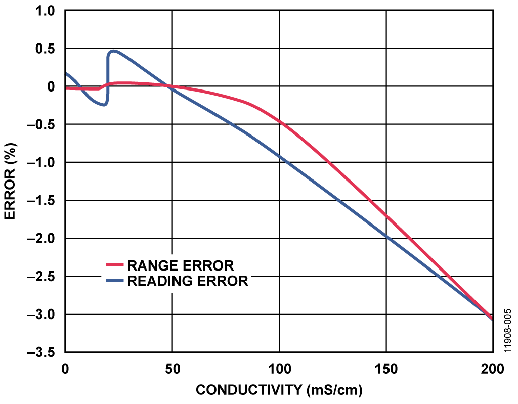
Table 3 shows the results of the high range measurements, and Figure 5 shows both the percent relative error of the range and the percent relative error of the reading. In the high range, from 0.2 mS to 200 mS, the percent error of the reading does not exceed 3%.
| RCELL (Ω) | YCELL (mS/cm) | YR (mS/cm) | RR (Ω) | % Error of Range | % Error of Reading |
| 0 | ∞ | 5255 | 0.1903 | Not applicable | Not applicable |
| 1 | 1000.0000 | 809.4 | 1.2355 | −95.3000 | −19.06 |
| 5 | 200.0000 | 193.9 | 5.1573 | −3.0500 | −3.05 |
| 10 | 100.0000 | 99.1 | 10.09 | −0.4500 | −0.90 |
| 20 | 50.0000 | 49.99 | 20.00 | −0.0050 | −0.02 |
| 50 | 20.0000 | 20.1 | 49.75 | +0.0500 | +0.50 |
| 100 | 10.0000 | 9.99 | 100.10 | −0.0050 | −0.10 |
| 200 | 5.0000 | 5.004 | 199.84 | +0.0020 | +0.08 |
| 500 | 2.0000 | 2.004 | 499.00 | +0.0020 | +0.20 |
| 1000 | 1.0000 | 1.001 | 999.00 | +0.0005 | +0.10 |
| 1300 | 0.7692 | 0.7681 | 1301.91 | −0.0006 | −0.15 |
| 2210 | 0.4525 | 0.4533 | 2206.04 | +0.0004 | +0.18 |
| 4700 | 0.2128 | 0.2116 | 4725.90 | −0.0006 | −0.55 |
| 6120 | 0.1634 | 0.1641 | 6093.85 | +0.0004 | +0.43 |
Table 4 shows the results from Table 3, with the resistive offset of 0.1903 Ω corrected. The RR column, corrected in Table 4 is obtained by subtracting 0.1903 Ω from the RR column in Table 3.
| RCELL (Ω) | YCELL (mS/cm) | YR (mS/cm) | RR (Ω) | RR (Ω) Corrected | YR (mS/cm) | % Error of Range | % Error of Reading |
| 0 | ∞ | 5255 | 0.1903 | 0.00 | Not applicable | Not applicable | Not applicable |
| 1 | 1000.00 | 809.4 | 1.2355 | 1.045 | 956.77 | −21.6149 | −4.323 |
| 5 | 200.00 | 193.9 | 5.1573 | 4.967 | 201.33 | +0.6644 | +0.664 |
| 10 | 100.00 | 99.1 | 10.09 | 9.901 | 101.00 | +0.5024 | 1.005 |
| 20 | 50.00 | 49.99 | 20.00 | 19.81 | 50.47 | +0.2351 | +0.940 |
| 50 | 20.00 | 20.1 | 49.75 | 49.56 | 20.18 | +0.0886 | +0.886 |
| 100 | 10.00 | 9.99 | 100.10 | 99.91 | 10.01 | +0.0045 | +0.090 |
| 200 | 5.00 | 5.004 | 199.84 | 199.65 | 5.01 | +0.0044 | +0.175 |
| 500 | 2.00 | 2.004 | 499.00 | 498.81 | 2.00 | +0.0024 | +0.238 |
| 1000 | 1.00 | 1.001 | 999.00 | 998.81 | 1.00 | +0.0006 | +0.119 |
| 1300 | 0.7692 | 0.7681 | 1301.91 | 1301.72 | 0.77 | −0.0005 | −0.132 |
| 2210 | 0.4525 | 0.4533 | 2206.04 | 2205.85 | 0.45 | +0.0004 | +0.188 |
| 4700 | 0.2128 | 0.2116 | 4725.90 | 4725.71 | 0.21 | −0.0006 | −0.544 |
| 6120 | 0.1634 | 0.1641 | 6093.85 | 6093.65 | 0.16 | +0.0004 | +0.432 |
The software (CN-0349 Evaluation Software) can make this correction. After correction, the 0.2 mS to 200 mS range has a percent error of less than 1% (see Figure 6).

Conductivity Measurements using Conductivity Cells
Table 5 shows the results of conductivity measurements on six 0.1% accurate standard KCl solutions: 0.1469 mS/cm, 0.2916 mS/cm, 0.7182 mS/cm, 1.408 mS/cm, 12.85 mS/cm, and 111.3 mS/cm.
| Measurement | Standard Cell Conductivity | Unit | |||||
| Standard KCl Solution (Conductivity Values) |
0.1469 | 0.2916 | 0.7182 | 1.408 | 12.85 | 111.3 | mS/cm |
| Conductivity Reading | 0.1471 | 0.2923 | 0.7215 | 1.415 | 12.93 | 109.8 | mS/cm |
| Error of Reading | 0.14 | 0.22 | 0.46 | 0.5 | 0.62 | 1.35 | % |
The conductivity cell used is a Sensorex CS200TC-PT1 with a cell constant equal to 1/cm and a built-in Pt100 RTD temperature sensor.
The standard KCl solutions were made in a specialized Bulgarian laboratory, and they were used as data points to check the system. When the cell constant of the conductivity cell is unknown, standard solutions can also be used as calibration points instead of calibration resistors.
More information about conductivity measurement and standard solutions can be found in Shreiner, R.H., and Pratt, K.W., Primary Standards and Standard Reference Materials for Electrolytic Conductivity (2004), NIST Special Publication 260-142.
PCB Layout Considerations
In any circuit where accuracy is crucial, it is important to consider the power supply and ground return layout on the board. The PCB must isolate the digital and analog sections as much as possible. The PCB for this system is constructed in a simple, 2-layer stack up, but 4-layer stack up gives better electromagnetic interference/radio frequency interference (EMI/RFI) performance. See the MT-031 Tutorial Tutorial for more discussion on layout and grounding, and the MT-101 Tutorial for information on decoupling techniques. Decouple the power supply of the AD8606 with a 10 μF capacitor and a 0.1 μF capacitor to properly suppress noise and reduce ripple. Place the capacitors as close to the device as possible, with the 0.1 μF capacitor having a low effective series resistance (ESR) value. Ceramic capacitors are advised for all high frequency decoupling. Power supply lines must have as large a trace width as possible to provide low impedance path and to reduce glitch effects on the supply line. The ADuM5000 and the ADuM1250 isoPower devices require power supply bypassing at the input and the output supply pins. Note that low ESR bypass capacitors are required as close to the chip pads as possible. A parallel combination of at least two capacitors is required to suppress noise and reduce ripple. The recommended capacitor values are 0.1 μF and 10 μF for VDD1 and VISO, which applies for both the ADuM5000 and the ADuM1250. The smaller capacitor must have a low ESR; for example, a ceramic capacitor. The total lead length between the ends of the low ESR capacitor and the input power supply pin must not exceed 2 mm. Installing the bypass capacitor with traces more than 2 mm in length may result in data corruption. For more information, see the ADuM5000 data sheet and the ADuM1250 data sheet.
A complete documentation package including schematics, board layout, and bill of materials (BOM) can be found at www.analog.com/CN0349-DesignSupport.
Setting Up and Programming
The EVAL-CN0349-PMDZ uses the CN-0349 Evaluation Software to perform calibration procedures and to capture data from conductivity cells. Figure 7 shows the calibration window of the software. Click Calibrate to initialize the calibration procedure. The software performs the three point calibration procedure automatically by controlling the ADG715 octal switch. To perform the calibration procedure properly, the three calibration resistance indicators must be previously filled in with the correct values. During the automatic calibration procedure, the software makes measurements in the three calibration points and stores the calibration coefficients (Gain Factor G and System Offset NOS) in the software memory, as described in the Calibration Procedure section. For the two measurement ranges, two different calibration coefficients are calculated and stored in the memory (G1 and G2, NOS1 and NOS2). When making a measurement, the corresponding gain factor and system offset is selected according to the chosen range.

Figure 8 shows the main window of the software, where different measurement results are presented. According to the chosen range, a measurement can be performed and values for the input impedance, conductivity, temperature, and conductivity temperature compensated are obtained. To display the results properly, data for the probe corrections must be properly selected.

The cell constant has to be the same as the one used for the measurements. For standard cells, this constant is usually between 0.01/cm and 10/cm.
The offset indicator is used for offset correction to alter the measurement by an offset value expressed in mS/cm.
The temperature coefficient must be chosen depending on the measured solution. When the value of this coefficient is set to 0%/°С, no temperature compensation is performed.
バリエーション回路
This circuit was proven to work with good stability and accuracy with the component values shown. Other precision op amps can be used in place of a dual version AD8606. Two single version AD8605 op amps can be used instead of the AD8606 to facilitate the PCB layout. The AD8608 is a quad version of the AD8605 and can be used as a substitute for the AD8606, if additional precision op amps are needed. The AD8601, the AD8602 and the AD8604 are single, dual, and quad rail-to-rail, input and output, single-supply amplifiers, featuring very low offset voltage and wide signal bandwidth, which can be used in place of the AD8605, the AD8606, and the AD8608.
The AD5933 impedance converter is similar to the AD5934 and combines an on-board frequency generator with a 12-bit, 1 MSPS ADC.
The ADM3260 is a hot swappable, dual channel I2C isolator with an integrated dc-to-dc converter that can be used in place of the ADuM5000 and ADuM1250 combination.
If galvanic isolation is not required, the power and the I2C lines can be connected directly to the microprocessor.
回路の評価とテスト
This circuit uses the EVAL-CN0349-PMDZ circuit board, the SDP-PMD-IB1Z, and the EVAL-SDP-CB1Z system demonstration platform (SDP) evaluation board. The SDP-PMD-IB1Z interposer board and the EVAL-SDP-CB1Z SDP board have 120-pin mating connectors. The SDP-PMD-IB1Z interposer board and the EVAL-CN0349-PMDZ board have 8-pin IMOD matching connectors, allowing quick setup and evaluation of the performance of the circuit. The EVAL-CN0349-PMDZ board contains the circuit to be evaluated, and the SDP evaluation board is used with the CN-0349 Evaluation Software to capture the data from the EVAL-CN0349-PMDZ circuit board.
Equipment Needed
The following equipment is needed:
- A PC with a USB port, Windows® 7 (64-bit), Windows 8 (64-bit), Windows 10 (64-bit), or Windows 8 (64-bit or 32-bit)
- The EVAL-CN0349-PMDZ circuit evaluation board
- The EVAL-SDP-CB1Z SDP evaluation board
- The SDP-PMD-IB1Z interposer board
- A 6 V power supply or wall wart (EVAL-CFTL-6V-PWRZ)
- The CN-0349 Evaluation Software
- A conductivity cell with integrated Pt100 sensor (for example, Sensorex CS200TC-PT1)
Getting Started
Load the evaluation software by placing the CN-0349 Evaluation Software CD into the PC. The user can also download the most up to date copy of the evaluation software from CN-0349 Evaluation Software. Using My Computer, locate the drive that contains the evaluation software CD and open the setup.exe. Follow the on-screen prompts to finish the installation. It is recommended to install all software components to the default locations.
Figure 9. Test Setup Functional Block Diagram
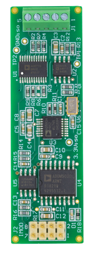
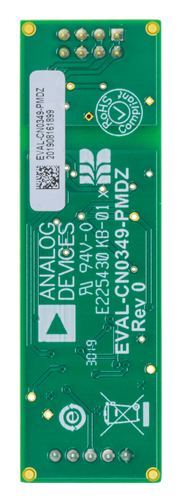
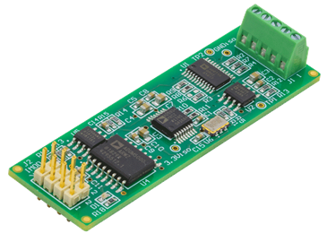
Figure 10. Photo of EVAL-CN0349-PMDZ Evaluation Board
Functional Block Diagram
See Figure 1 for the circuit block diagram and see the EVAL-CN0349-PMDZ-Altium DesignerSchematic.pdf file for the circuit schematics. This pdf file is located in the CN-0349 Design Support Package. A block diagram of the test setup is shown in Figure 9.
Setup
For proper setup, take the following steps:
- Connect the EVAL-CFTL-6V-PWRZ (6 V dc power supply) to the SDP-PMD-IB1Z interposer board via the dc barrel jack.
- Connect the SDP-PMD-IB1Z interposer board to the EVAL-SDP-CB1Z SDP board via the 120-pin Connector A.
- Connect the EVAL-SDP-CB1Z SDP board to the PC via the USB cable.
- Connect the EVAL-CN0349-PMDZ evaluation board to the SDP-PMD-IB1Z interposer board via the 8-pin header IMOD connector cable supplied with the CN-0349 board (4-pin MTE cable, Digilent, Inc.).
Connect the conductivity cell to the EVAL-CN0349-PMDZ evaluation board via the J1 terminal block. A photo of the EVAL-CN0349-PMDZ board is shown in Figure 10.
Test
Launch the CN-0349 Evaluation Software. The software will be able to communicate with the SDP board if the Analog Devices SDP drivers are listed in the Device Manager. When USB communications are established, the SDP board is used to send, receive, and capture serial data from the EVAL-CN0349-PMDZ board. Data, information, and details regarding how to use the evaluation software for data capturing can be found in the CN-0349 Software User Guide.
