Overview
Design Resources
Design & Integration File
- Schematic
- Bill of Materials
- Gerber Files
- PADS Files
- Assembly Drawing
Evaluation Hardware
Part Numbers with "Z" indicate RoHS Compliance. Boards checked are needed to evaluate this circuit.
- EVAL-CN0290-SDPZ ($243.64) Extending the Low Frequency Range of a High Performance Phase Locked Loop
- EVAL-SDP-CS1Z ($66.32) Eval Control Board
Device Drivers
Software such as C code and/or FPGA code, used to communicate with component's digital interface.
Features & Benefits
- Phase locked loop with extended low frequency range
- LO down to 10MHz, RF down to 100MHz
- Low distortion and phase noise
Markets and Technologies
Parts Used
Documentation & Resources
-
AN-586: LVDS Outputs for High Speed A/D Converters (Rev. 0)2/14/2015PDF207 kB
-
AN-30: Ask the Applications Engineer - PLL Synthesizers12/6/2004PDF184 kB
-
Fundamentals of Phase Locked Loops (PLLs)2/14/2015PDF407 kB
-
MT-101: Decoupling Techniques2/14/2015PDF954 kB
-
MT-031: Grounding Data Converters and Solving the Mystery of "AGND" and "DGND"3/20/2009PDF144 kB
-
CN-0290: Extending the Low Frequency Range of a High Performance Phase Locked Loop9/24/2013PDF311 kB
Circuit Function & Benefits

For example, the minimum reference frequency and the RF input frequency of a number of Analog Devices PLLs, such as the ADF4106, are specified for 20 MHz and 500 MHz, respectively. The frequency range can be lowered to a 10 MHz reference frequency and a 100 MHz RF input using the additional clock buffers as in Figure 1.
Circuit Description
The ADF4106 frequency synthesizer can be used to implement the local oscillator function in the up-conversion and down-conversion sections of RF receivers, transmitters, signal analyzers, data generators, or any RF application that requires a local oscillator function. A complete phase-locked loop (PLL) is realized when the synthesizer is used with an external loop filter and voltage controlled oscillator (VCO).
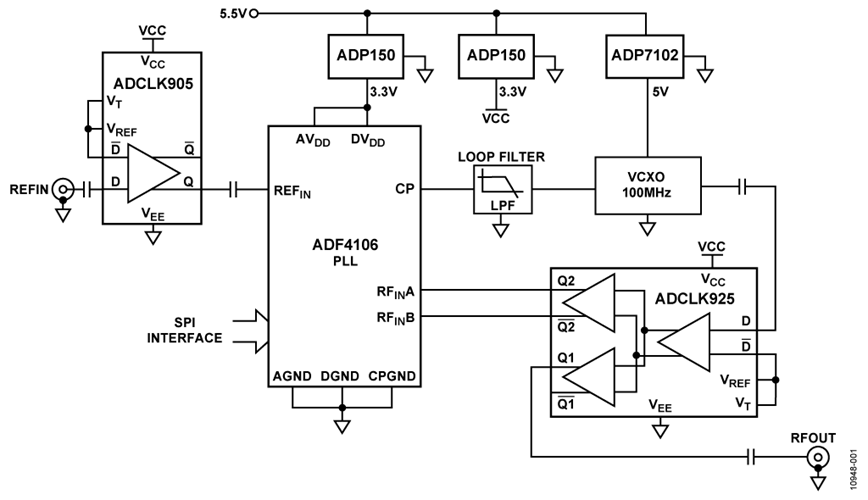
The ADF4106 is an integer-N PLL where the channel step size is an integer number N. This device has an RF frequency output range up to 6 GHz, is easy to use, and is specified for low phase noise, typically −223 dBc/Hz (normalized phase noise floor ). Figure.1 shows the block diagram, and Figure 2 shows the simplified schematic of a complete phase locked loop using the ADF4106 in a low noise single frequency clock application.

A low noise 10 MHz reference source is buffered by the ADCLK905 and ac coupled to the REFIN of the ADF4106 PLL. The VCO is a low noise, 100 MHz sinewave VCXO, whose output is ac coupled to the 50 Ω input load of the ADCLK925. Interfacing between the VCXO and the ADCLK925 is very simple, as both devices are matched in terms of their load and signal level requirements. The ADCLK925 1:2 buffer output stage provides both and the RFOUT signal and the required RF feedback signal to the PLL.
The ADF4106 PLL is powered from a dedicated 3.3 V ADP150 low noise LDO, and the two clock buffers (ADCLK905, ADCLK925) are powered using a second ADP150. The ADP150 has an output voltage noise of only 9 μV rms, which ensures low phase noise for both the PLL and the clock buffers.
The low noise VCXO is powered from the ADP7102 low noise 5 V linear regulator to reduce the impact of VCO pushing (equivalent to power supply rejection).
Reference Input Clock Buffer
The clock buffers for the REFIN and the RFIN input stages of the PLL need to have low additive jitter, sufficient slew rate at the frequency of operation, and adequate signal swing to match the ADF4106 requirements.
The ADCLK905/ADCLK925 are ultrafast ECL clock/data buffers, designed specifically to minimize added random jitter over a wide input slew rate. They feature full-swing ECL emitter coupled logic output drivers, 95 ps propagation delay and 60 fs random jitter. The rise/fall time (20% to 80%) of these parts is 60 ps typical which corresponds to a slew rate of approximately 8000 V/μs.
The ADCLK905 is used to buffer the 10 MHz REFIN frequency source. A reference frequency of 10 MHz is common in many applications. Depending on the signal swing available, the slew rate may not meet the minimum 50 V/μsec slew rate requirement of the ADF4106. For example, the slew rate of a 10 MHz 0 dBm sine wave is only 20 V/μs.
The ADCLK905 was chosen as the REFIN clock buffer in order to increase the slew rate of the 10 MHz source. The ADCLK905 low additive jitter ensures that any additive jitter introduced by the REFIN clock buffer is minimal. Reference noise within the bandwidth of the PLL is not attenuated, therefore keeping the reference noise low, is a key factor in component choice. The low 60 fs additive jitter of the ADCLK905 ensures that this is the case. In a 50 Ω environment, input and output matching have a significant impact on performance. The input buffer of the ADCLK905 provides internal 50 Ω termination resistors for both D inputs. The center tap, VT, between these 50 Ω resistors is connected externally to the complementary D input and to the VREF pin. These pins are decoupled with a ceramic capacitor.
The PECL output stage of the ADCLK905 directly drives 800 mV each side into 50 Ω terminated to VCC − 2 V. The termination is implemented with a single resistor termination to each ADCLK905 output. For VCC = 3.3 V, 150 Ω connected to ground is the recommended value.
The outputs are designed to drive transmission lines, and each output pin should see matched load impedances. The ADCLK905 Q output is ac coupled to a 50 Ω load, before ac coupling to the high impedance input of the ADF4106 REFIN. The unused complementary Q output should be terminated with a similar load.
RF Input Clock Buffer
The ADCLK925 is used to buffer the 100 MHz RFIN from the low noise VCXO. The RFIN has a required minimum slew rate of 320 V/μsec. The ADCLK925 provides the required slew rate at the RFIN input. The low additive jitter of the ADCLK925 has minimal impact on the PLL phase noise performance. The 1:2 output stage of the ADCLK925 simplifies feedback to the PLL without the need for a splitter and matching components.
The PECL output stages directly drives 800 mV each side into 50 Ω terminated to VCC − 2V. This is achieved without the need for an additional supply by using a single 150 Ω resistor to ground, as shown in Figure 2. The RFIN input stage of the ADF4106 is specified for a maximum signal level of ± 600 mV. A series resistor of 30 Ω reduces the ADCLK925 output swing to below this value. The ADCLK925 output is ac coupled to the differential 50 Ω input of the ADF4106 The second ADCLK925 output is terminated in a similar manner and provides the RFOUT signal.
PLL Design and Performance
The ADIsimPLL™ software was used to design the loop filter of the PLL using the required low frequency values of 10 MHz REFIN and 100 MHz RFIN. The loop filter has 818 Hz bandwidth and 45° phase margin.
Figure 3 shows the ADIsimPLL simulated phase noise and indicates that the ADF4106 PLL loop locks at low frequency with a minimum increase in phase noise.
The actual measured phase noise of the PLL system is shown in Figure 4.

The ADIsimPLL software used to generate the loop filter components can also be used to simulate the performance of the circuit. ADIsimPLL assumes an adequate signal slew rate and signal swing is provided by the REFIN and RFIN inputs. ADIsimPLL allows modeling the reference source used by the ADF4106 PLL, which for this setup is the R&S SMA100 signal generator. The phase noise of the single-ended 10 MHz, 0 dBm reference input signal was modeled using the measured values at offsets of 10 Hz and 1 MHz. The Agilent FSUP spectrum analyzer was used to measure the reference phase noise at these offsets. In order to simulate the VCO performance in ADIsimPLL, it is necessary to combine the phase noise from both the ADCLK925 datasheet and the CVSS-945 VCXO (Crystek Crystals, 12730 Commonwealth Drive, Fort Myers, Florida 33913) as shown in Table 1.
Table 1. Combined Phase Noise
| Phase Noise Offset | ADCLK925 (dBc/Hz) | VCXO (dBc/Hz) | Total (dBc/Hz) |
| 10 Hz | −140 | −86 | −86 |
| 1 MHz | −158 | −172 | −157 |
The combined 1/f phase noise is −86dBc/Hz at 10 Hz offset. The −140 dBc value at 10 Hz offset from the ADCLK925 datasheet will have negligible effect on the combined 1/f phase noise.
The combined phase noise is −157 dBc/Hz at an offset of 1 MHz.
The ADCLK925 phase noise at 1 MHz offset in the data sheet is –161 dBc/Hz. This is measured differentially, so it is necessary to adjust the datasheet measured noise floor by 3 dB when using a single-ended output. The VCXO phase noise of −172 dBc/Hz has an almost negligible contribution to the combined phase noise.
Comparison of Measured vs. Simulated Results
Table 2 shows simulated and measured results for phase noise and phase jitter. The phase noise is measured at offsets of 100 Hz, 2 kHz, and 100 kHz. Phase jitter is integrated from 100 Hz to 30 MHz. The ADIsimPLL program in this simulation uses a point floor model for the reference and VCO. As a result, the models in ADIsimPLL match very closely to the 1/f noise and the noise floor, but they can differ by several dB at intermediate offsets from the carrier.
Table 2. ADF4106 PLL System Simulated and Measured Phase Noise and Phase Jitter
| Parameter | Simulated | Measured |
| PN Offset of 100 Hz | −113 dBc/Hz | −114 dBc/Hz |
| PN Offset of 2 kHz | −126 dBc/Hz | −122 dBc/Hz |
| PN Offset of 100 kHz | −156 dBc/Hz | −156 dBc/Hz |
| Phase Jitter (100 Hz to 30 MHz) | 208 fs | 276 fs |
Common Variations
Other buffers such as the ADCMP600 high speed CMOS comparator can be used to increase the slew rate for the REFIN circuit, however the additive jitter should be evaluated for the application in question.
All additional components will introduce some amount of additive noise, which can degrade the in-band phase noise and phase noise jitter. This may be acceptable for some applications, where the degradation in phase noise performance is still within the acceptable limits.
The ADCLK9xx, family of clock buffers have very low additive jitter, however low slew rate signal inputs will degrade this specification. The ADCLK9xx data sheets should be consulted to evaluate this degradation.
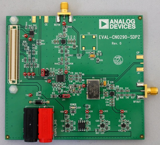
A photo of the EVAL-CN0290-SDPZ circuit board is shown in Figure 5.


Figure 6. Measurement Setup for Phase Noise and Phase Jitter Testing
Circuit Evaluation & Test
- PC with a USB port and Windows® XP, Windows Vista® (32-bit), or Windows® 7 (32-bit)
- EVAL-CN0290-SDPZ circuit evaluation board
- EVAL-SDP-CS1Z SDP evaluation board
- Integer-N v7 or greater evaluation software
- Power supply: +5.5 V.
- RF signal source (R&S SMA100 or equivalent)
- Spectrum Analyzer (Agilent FSUP or equivalent)
- Coaxial RF cables with SMA connectors
Refer to the UG-582 User Guide for software installation and test setup. The design support package includes the schematics, layout files, and the bill of materials (www.analog.com/CN0290-DesignSupport). For additional details, refer to the ADF4106, ADCLK905, and the ADCLK925 data sheets.
Refer to Figure 1 of this circuit note for the block diagram and Figure 2 for simplified schematic. A block diagram of the test setup is shown in Figure 6.
After setting up the equipment, use standard RF test methods to measure the phase noise and phase jitter of the circuit.


