Abstract
Mixed-signal front-end (MxFE®) products are enabling the latest software designed radio solution with a very wide 7.5 GHz bandwidth. The digital-to-analog converter (DAC) and analog-to-digital converter (ADC) cores of the MxFE use sampling clocks that originate from either the internal phase-locked loop (PLL) or an external clock source. Determining the clock solution is quickly determined using a PLL synthesizer design and simulation tool such as ADIsimPLL™. Designers using the MxFE can now take advantage of the MxFE models recently available in ADIsimPLL to design the high performance sampling clock required for the radio solution, where key performance specifications can be measured, loop filters are optimized, and PLL parameters are adjusted. This article describes the use of this software to model the on-chip PLL and VCO integrated in the MxFE and radio frequency DAC (RFDAC).
Introduction
Selecting the right components for clock generation enables a designer to extract the best performance from the configured platform.
Important criteria to consider when choosing a clock generator are phase jitter and phase noise floor, which impact the signal-to-noise ratio (SNR) of the data converter being clocked.
Analog Devices’ MxFE family of devices and AD917x RFDACs all contain on-chip integer type PLL synthesizers to generate the DAC and ADC sampling clocks. Depending on the application, the phase noise/integrated jitter performance of the on-chip PLL/VCO synthesizer locked to the input reference can be sufficient to meet the application requirements. In some applications, an external clock source with lower phase noise may be required to be used instead of the on-chip PLL/VCO integrated. Modeling the phase noise/jitter performance by the ADIsimPLL software enables the designer to make this decision at an early stage in the development process.
Using the ADIsimPLL software, configured to model the desired integrated PLL/VCO with the available reference also modeled, the phase noise and integrated jitter results are generated. Adjustments to the on-chip charge pump current and external loop filter components can be modeled in ADIsimPLL to determine optimum values. Modeling the available reference source to be used by the software allows the designer to quickly determine the effect of the reference noise on the sampling clock and so eases the selection process of the reference clock.
This article illustrates how to use the ADIsimPLL software to design and simulate the clock source for the MxFE family of devices using the AD9081 model in the software, but the process is the same for all the MxFE devices and the AD917x RFDACs. The model illustration included herein uses an input reference frequency of 500 MHz to design a PLL with a VCO frequency of 12 GHz. Creating a model for this 500 MHz reference source for use within the ADIsimPLL software is also described. Included is a comparison between the ADIsimPLL model phase noise/rms jitter results for the sampling clock with that of a measured laboratory sampling clock using the evaluation board platform for the MxFE device.
MxFE Sampling Clock Design Example
To create the MxFE sampling clock design, you can download the ADIsimPLL design tool from analog.com/ADIsimPLL.
Once installed, to begin the design process, open ADIsimPLL.
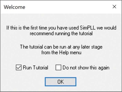
Figure 1. The ADIsimPLL welcome screen.
Close the tutorial.
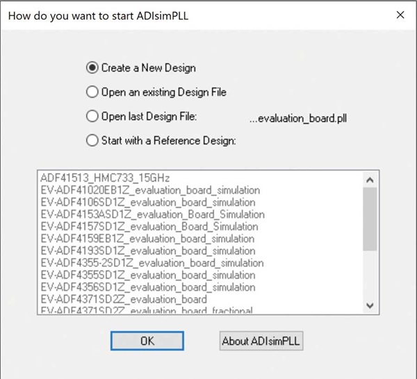
Figure 2. Starting a new design in ADIsimPLL.
Select Create a New Design.
Click OK.

Figure 3. New PLL wizard.
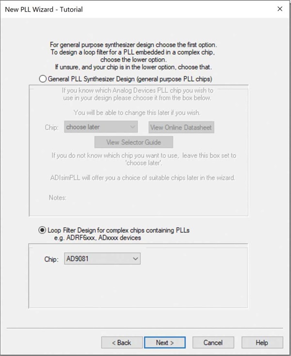
Figure 4. Select the loop filter design for the AD9081.
Select the Loop Filter Design for complex chips containing PLLs.
Select the AD9081 from the Chip dropdown options.
Click Next to configure the PLL synthesizer in the AD9081.
The graphical configuration page shows the block diagram of the PLL and significant registers, frequencies, and design options. On this page, you can choose from a range of standard configurations or alter registers and other options directly to configure the device.
Here you can directly input data to the boxes surrounded in green, and the other cells update automatically. Counter values can be altered by hovering the cursor over the cell and using the mouse wheel. Options can be selected using dropdown lists. Frequency and register limits are checked in real time and errors are displayed in red, along with error messages.

Figure 5. Configure the PLL for the AD9081.
To simulate for fDAC = 12 GHz, simply change the DACCLK Freq green box to 12 GHz. The CLKIN Freq is by default = 500 MHz.

Figure 6. The PLL configured for the AD9081.
Click Next.
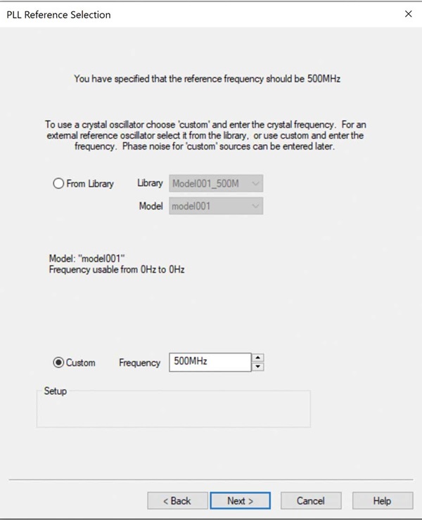
Figure 7. The PLL reference selection.
To use measured phase noise data of the Reference/CLKIN oscillator, you must place this data in a library file using the Reference Library Editor. You can then select this model From Library. Refer to the ADIsimPLL Reference Model Creation section in this article for details on using this editor.
Click Next.
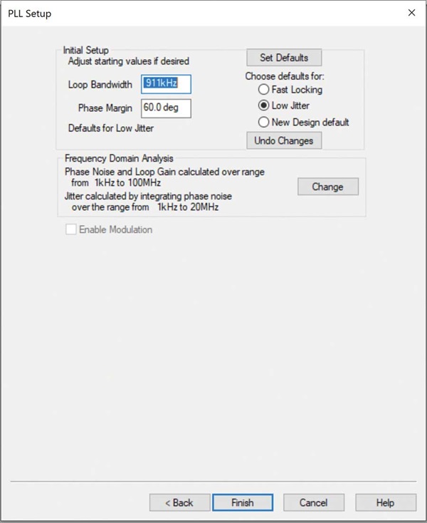
Figure 8. The PLL setup.
Choose the defaults for fast locking or low jitter and click Finish.
The Report tab of the PLL synthesizer design prints the frequency domain analysis at 12 GHz and phase jitter using a brick wall filter. By selecting the tabs at the bottom of the screen, you can navigate directly to the Components, FreqDomain, Schematic, and DACn elements of the PLL synthesizer model.

Figure 9. The ADIsimPLL report tab.
The Components tab allows you to look at the VCO phase noise and the reference phase noise at the analysis frequency, which is 12 GHz. The VCO phase noise plot represents the phase noise from the VCO measured in a free running configuration (that is, unlocked—not in a PLL) at 12 GHz. When the VCO is locked in a PLL, the output phase noise is reduced significantly at frequencies inside the PLL loop bandwidth. The Reference/CLKIN phase noise represents the phase noise from the reference source. The reference phase noise affects the output phase noise of the PLL, primarily inside the loop bandwidth.

Figure 10. The ADIsimPLL components tab.
By default, the reference phase noise is modeled as having a phase noise of None. In order to add reference noise, you can change the reference phase noise from None to Point/Floor (as shown in Figure 11), to Corner/Floor, or to Leeson. Point/Floor specifies the phase noise at one point and the phase noise (PN) floor, Corner/Floor specifies the phase noise floor and corner frequencies, and Leeson specifies oscillator parameters such as power, noise figure, and loaded Q.
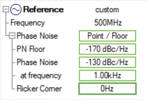
Figure 11. Reference phase noise options.
The FreqDomain tab displays the open-loop gain and phase, and the output phase noise of the model. The output phase noise represents the phase noise from the VCO measured when locked in the PLL. This includes contributions from all noise sources within the PLL. By expanding the FreqDomain folder in the data panel on the left, the min or max frequency of the plot can be changed as required.

Figure 12. The ADIsimPLL FreqDomain tab.
The Schematic tab shows a simplified schematic of the synthesizer.

Figure 13. The ADIsimPLL schematic tab.
Expanding the Loop Filter folder in the data panel allows you to modify the loop filter components to match an existing schematic such at the evaluation board schematic. The loop filter components in the Schematic can be changed by specifying Components and changing the values as shown in Figure 14.
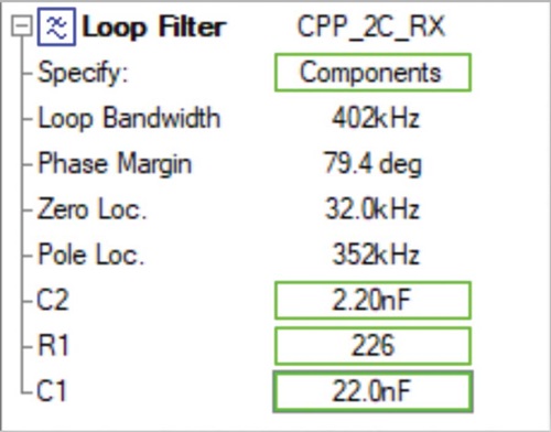
Figure 14. Loop filter components.
The DACn tab allows us to look at the phase noise of the DAC output. The plot in Figure 15 models the DAC output at 3 GHz by selecting the DDS div option of 4. Noninteger DDS div values can also be selected. The marker is enabled to read the phase noise.

Figure 15. The ADIsimPLL DACn tab.
ADIsimPLL Reference Model Creation
The reference model is created using the Reference Library Editor. From the main menu choose Libraries/Reference Library Editor to start the desired type of editor.
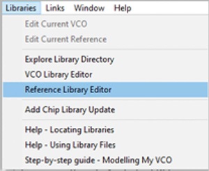
Figure 16. The Reference Library Editor.
Select New as highlighted in Figure 17.

Figure 17. Reference Library Editor New Model.
Choose a Model Name.

Figure 18. Reference Library Editor new model name edit.
Select table from the menu on the left. Then input the reference frequency and PN floor used.
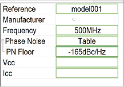
Figure 19. Reference frequency and phase noise floor.
Then select Phase Noise Table and properties from the top menu.
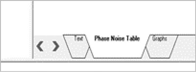
Figure 20. Reference Phase Noise Table Select.
Select Change Number of Rows. Then change the number to match the measured phase data number of points and press OK.

Figure 21. Reference Phase Noise Table properties.
Then enter the measured phase noise data of the reference to the table. The first entry of each pair is assumed to be the offset frequency and the second the phase noise at that frequency. The offset frequency entries must increase.

Figure 22. Reference Phase Noise Table data entry.
Press Save on the top left and save within the reference folder. See Figure 16.
The model should then be available in the library for selection when creating a new design.
Measured vs. Model Simulation
In order to determine the accuracy of the ADIsimPLL model data with measured results, the AD9081-EBZ evaluation platform was configured to generate a DAC output at 3 GHz using an fDAC = 12 GHz. The plots in Figure 23 and Figure 24 show measured phase noise (in blue) vs. ADIsimPLL model phase noise (in red) for the default charge pump current (ICP) = 2 mA and the maximum ICP = 6.4 mA.

Figure 23. The AD9081 phase noise, fDAC = 12 GHz, DAC output = 3 GHz, ICP = 2.0 mA.

Figure 24. The AD9081 phase noise, fDAC = 12 GHz, DAC output = 3 GHz, ICP = 6.4 mA.
Conclusion
The current version of ADIsimPLL available from ADI includes models for the MxFE and the AD917x RFDAC (RF high speed DACs). Using the models in ADIsimPLL significantly reduces the time required to design the sampling clock. As shown in this article, the performance results provided by the MxFE models match closely to actual bench measurements, making this modeling tool a useful and worthwhile process to use prior to schematic entry.

