CN0561

Overview
Design Resources
Design & Integration File
- Schematic
- Bill of Materials
- Assembly Files
- Gerber Files
- CAD Layout
Evaluation Hardware
Part Numbers with "Z" indicate RoHS Compliance. Boards checked are needed to evaluate this circuit.
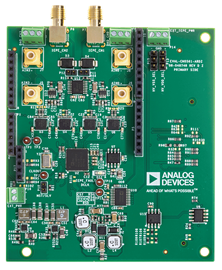
- EVAL-CN0561-ARDZ ($228.85) Alias Free 24-bit, Quad Channel Wide Bandwidth Data Acquisition System for IEPE Sensor with Fault and Sensor protection
Device Drivers
Software such as C code and/or FPGA code, used to communicate with component's digital interface.
LTC6373 GitHub Linux Driver Source Code
AD713x GitHub no-OS Driver Source Code
FPGA/HDL
Features & Benefits
- Alias Free Quad Channel data acquisition
- Alias free dual IEPE-Compatible Vibration Sensor Interface
- Channel Independent Excitation Source and Sensor Bias
- Analog Overvoltage and Undervoltage Protection
- Sensor Frequency Response from DC up to 54 kHz
- Synchronized, Full Bandwidth Data Measurement and Capture
Documentation & Resources
-
CN0561 User Guide (Wiki)7/3/2025WIKI
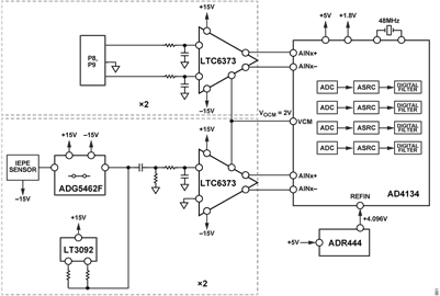
Circuit Function & Benefits
The reference design shown in Figure 1 shows an alias free, high resolution, wide bandwidth, high dynamic range, integrated electronics piezoelectric (IEPE)-compatible interface data acquisition (DAQ) system that interfaces with IC Piezoelectric (ICP®)/IEPE sensors. The most common IEPE sensors are usually found in applications measuring vibration, but there are many IEPE sensors that measure parameters such as temperature, strain, shock, and displacement.
The focus of this circuit note is on the application of this solution to multichannel or multiaxis vibration measurements for advanced condition based monitoring applications. However, there is a large set of applications in instrumentation and industrial automation that use IEPE sensors in a similar way and that are served by similar signal chains.
Condition-based monitoring, in particular, uses sensor information to predict changes in the condition of a machine. While there are many methods of tracking the condition of a machine, vibration analysis is the most commonly used method. By tracking the vibration analysis data over time, a fault or failure can be predicted, along with the source of the fault.
Vibration sensing in an industrial environment presents additional challenges because of the need for robust and reliable sensing methods. Knowing the condition of a machine helps increase efficiency, productivity, and creates a safer working environment.
The AD4134 reference design is an AC-coupled solution in which by looking at the complete data set from an IEPE vibration sensor in the frequency domain (dc to 390kHz). The type and source of a machine fault can be better predicted using the position, amplitude, and number of harmonics found in the fast fourier transform (FFT) spectrum.
Circuit Description
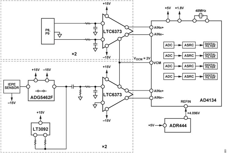
The circuit shown in Figure 1 is a sensor to bits (data acquisition) alias free signal chain for an IEPE sensor, consisting of a current source, instrumentation amplifier, protection circuit, and a fully differential alias free continuous time ADC. The IEPE interface is present on two channels, while the remaining 2 channels can be used for general 24-bit alias free data acquisition. The circuit consists of current source, quad channel protector, instrumentation amplifier, and fully differential sigma delta ADC.
The programmable current source, LT3092, drives the piezoelectric accelerometer with constant current. The output current can be programmed by external resistors and is usually set between 2mA and 20mA, depending on the type of sensor and the cable.
The signal output from the IEPE sensor is AC-coupled to the instrumentation amplifier, whose output is differential signal centered at 2V common-mode. This output is a fully differential voltage optimized for driving the ADC.
The AD4134 is an alias free continuous time sigma delta ADC with resistive input, hence there is no requirement of anti-aliasing filter or a fully differential amplifier. This helps reduce the signal chain size, noise, and phase delays, allowing for precision compact measurements. While piezoelectric accelerometers have bandwidths as high as 30kHz, a wider bandwidth signal chain is chosen with respect to phase delay, thereby achieving better phase matching performance in 2-axis measurements. Further bandwidth limiting occurs in the digital filter of the ADCs; however, the phase delay is known and deterministic.


ICP/IEPE ACCELEROMETER
Any IEPE vibration sensor can be interfaced with the AD4134 reference design because all the IEPE vibration sensors work using the same principle with different offset voltages, noise levels, bandwidths, and sensitivities. An IEPE output signal carries both ac and dc voltages, where the vibration dependent ac voltage is dc shifted to a voltage level between 7V and 13V. This dc level varies from sensor to sensor, and for any given sensor, it has a drift component with respect to time, temperature, and excitation current.
The IEPE sensor must be powered by a current source with a sufficiently high voltage range to fully cover the amplitude of the sensor. A typical excitation voltage of the IEPE sensors is 24V.
The input of the signal chain can receive a signal amplitude of up to 10V p-p with an offset voltage of up to 13V. The dc offset is removed by Series capacitor.


Figure 2 shows an ICP accelerometer block diagram of a sensor powered by a constant current source and connected to a dc-coupled signal chain. The maximum bandwidth of the sensor is proportional to the excitation current and inversely proportional to cable capacitance. The maximum desired output voltage of the sensor and cable type must be taken into account when choosing the level of the constant current, which can be determined by using the following equation:

where:
fMAX is the maximum frequency of the sensor in hertz.
IC is the constant current in mA.
1 mA is the power requirement of the sensor.
C is cable capacitance in pF.
V is the maximum peak voltage output from the sensor in volts.
Note that in Equation 1, 1mA is subtracted from the total current supplied to the sensor (IC), where the approximate 1mA powers sensor itself, and the rest of the current drives the cable. This number varies from sensor to sensor.
For example, this reference design is tested using an ICP accelerometer produced by PCB piezotronics, model 333B52 with a maximum peak output of 10V, a 10-foot cable length with a capacitance of 29pF/ft, and an excitation current of 2.5mA. Applying Equation 1, the maximum theoretical bandwidth of the sensor is 82.3kHz.
Neither the cable nor the chosen current level limit the performance of the sensor.
CONSTANT CURRENT SOURCE
Take care when designing the constant current source (CCS) and when considering noise performance. Low current noise is essential because current noise is converted to voltage noise when driving the input impedance of the signal chain.


Figure 3 depicts a 2-terminal current source with resistors RSET and ROUT setting the output current to 2.5mA, and capacitor CSET limiting the bandwidth of the current noise. The internal 10μA reference current source of the LT3092 holds a stable VSET across RSET. The VSET is mirrored across ROUT, which sets the output current according to Equation 2.

Note that the actual IOUT current is 10μA larger than the output current given by Equation 3 because of the internal reference current flowing from the SET terminal.
The data sheet recommends RSET = 20kΩ to set the voltage drop across RSET to 200mV, minimizing the effect of the offset voltage. (The offset voltage is more significant across a smaller VSET.) The white current noise produced by a resistor is given by Equation 3.

where:
T is absolute temperature in Kelvin.
k is Boltzmann’s constant in (J/K).
R is resistance.
Because resistor current noise is proportional to the square root of the inverse of resistance, increasing the value of RSET from the recommended 20kΩ to 120kΩ requires a proportional increase in ROUT as well (to keep the output current at the same level), causing a drop in the overall noise current. A capacitor, CSET, across RSET is recommended to lower the current noise of RSET and of the internal current reference of the LT3092. The CSET capacitor bypasses the current noise emitting from the LT3092.
An LT spice simulation of the constant current source, as shown in Figure 3, was performed to optimize component values and placement dependency. A non ideal voltage source was modeled, providing 0.7mV rms voltage noise and 224nA rms of current noise in a 20MHz bandwidth, simulating a keysight E3631 bench power supply with two outputs connected in series, set to 26V total.
Table 1 lists rms noise for various combinations of component values. The rms current noise is simulated for a bandwidth from 1MHz to 100kHz. CCOMP acts like a high-pass filter, passing the noise from the voltage source to the output. Further increasing RSET and ROUT helps in the current noise reduction, but it also causes a higher voltage drop over the resistors, reducing the allowable signal swing.
| RMS Noise (nA) | RSET (kΩ) | ROUT (Ω) | CSET | CCOMP |
| 158.8 | 20 | 80.6 | None1 | None1 |
| 1273.5 | 20 | 80.6 | None1 | 100 nF |
| 202.7 | 20 | 80.6 | None1 | 10 nF |
| 15.5 | 20 | 80.6 | 100 nF | None1 |
| 14.5 | 20 | 80.6 | 10 μF | None1 |
| 3.1 | 120 | 470 | 10 μF | None1 |
1 No component required.
When using a long cable with a high level of inductance, stability may become an issue. For more information on compensating inductive loads, refer to the LT3092 data sheet.
To calculate the usable sensor excitation voltage provided by the current source, use the following equation:

where:
VDD is the supply voltage of the constant current source.
LT3092DROP is the dropout voltage over the IC itself (typically 1.2V
at load current up to 10mA).
RSET × 10μA gives the dropout voltage over the resistor, which sets
the output current level and a current from the internal 10μA flows
through the resistor.
In this case, the usable excitation voltage is 23.6V.
INPUT PROTECTION CIRCUIT
The IEPE sensors are typically connected to the DAQ system via long cables. In an environment where many cables and other signal types are present, it is important to protect the DAQ system from any overvoltages that may occur due to operator miswiring or cable damage. The ADG5462F is a user defined input protection switch that automatically detects overvoltage conditions and open circuits the sensor from the data acquisition signal path. For the switches to be active, input signal levels from the sensor must be within the voltages on POSFV and NEGFV Pins. Note that VSS is the negative power supply pin and VDD is the positive power supply pin. The ADG5462F also provides a fault flag (FF) that can be used as an interrupt into a controller to alert the operator that an input fault has occurred. In normal operation, the FF pin is pulled high. However, if any of the Sx pin goes beyond positive fault voltage (POSFV) or negative fault voltage (NEGFV), the FF pin is pulled low to indicate a fault has occurred. If a fault is detected in the AD4134, the sensor input and current source disconnects from the data acquisition system.
ANALOG-TO-DIGITAL CONVERSION
The AD4134, a precision, quad channel, 24-bit, Continuous time Σ-Δ ADC has been chosen for its excellent dc to 390kHz bandwidth precision and the inherent alias free behavior.
The output data rate (ODR) of the ADC can either be programmed (SRC mode) in the AD4134 or set using a continuous external signal (ASRC mode) at the desired sampling speed.
In SRC mode for an ODR to be 375kSPS, calculate the decimation rate as follows:
Decimation Rate = 24MHz/375kHz = 64 = 0x00004000000000
Program ODR_VAL_INT, Bits[23:0] with 0x000040. Program
ODR_VAL_FLT, Bits[31:0] with 0x00000000.
Every time the ODR_VAL_INT, Bits[23:0] and ODR_VAL_FLT, Bits[31:0] are changed, the Bit 0 in the TRANSFER_REGISTER must be set to update the ODR to the new value.
The default settings for this reference design are optimized for an ADC measurement bandwidth of 32kHz, as follows:
- Conversion length: 24 bits
- ASRC mode
- High performance mode
- Status header enabled
| ADC Power Mode | Filter Type | ODR (kSPS) | −3dB Bandwidth (kHz) | RMS Noise (μV) |
| High | FIR | 128 | 55.4 | 6.03 |
| High | FIR | 64 | 27.7 | 4.68 |
| Low power | FIR | 128 | 55.4 | 11.15 |
| Low power | FIR | 64 | 27.7 | 7.59 |
| High Performance Mode, ODR = 64 kSPS | Low power mode, ODR = 64 kSPS | |||
| Condition | Dynamic Range (dB) | Noise (μV rms) | Dynamic Range (dB) | Noise (μV rms) |
| Shorted Input | 105.9 | 23.8 | 104.5 | 24.2 |
MEASURED PERFORMANCE OF THE SIGNAL CHAIN
This signal chain design targets medium to wider bandwidth vibration sensing, where higher harmonics and frequency content above 1kHz are important. In the design, there is a necessary trade-off between the system bandwidth, linearity, and the achievable noise performance. A higher input impedance is chosen to maintain signal accuracy (linearity), which in this design sets a maximum noise performance limit. The signal bandwidth is also set wider that the response of the system over higher frequencies is maintained. A lower noise solution can be achieved with a design that has a narrower bandwidth, thus removing more of the wideband noise.
Noise
Noise performance of the entire signal chain is measured with inputs shorted. Table 3 details the typical noise performance of the signal chain, without any sensor connected.
Figure 4 shows the dynamic range of the dc-coupled solution with shorted input over temperature.


Sensor Noise Contributions
The usual aim of the designer of a data acquisition system is to capture the sensor output signal as accurately as possible. In practice, this means that the performance of the system must be set by the sensor characteristics. The noise performance of the sensor is often one of the key limiting factors of the overall measurement system; understanding this helps to set the performance requirement of the design. For this design, the target is to support sensors that provide vibration data at bandwidths greater than 1kHz, which are used in data acquisition systems targeted at condition-based monitoring for predictive maintenance on rotating or reciprocating plant equipment. Table 4 details the performance level and bandwidth of a small selection of vibration sensors. The main considerations in sensor selection are typically bandwidth, range, noise spectral density (NSD), and power. The ADXL1002 and ADXL1004 sensors are low power devices suitable for a range of vibration applications, where power and bandwidth are important. These accelerometers are suitable for continuous monitoring applications, such as internet of things (IoT) machine monitoring.
For the highest sensitivities and bandwidths, where low noise and sensitivity at higher frequencies are key, piezoelectric sensors are still the most appropriate sensors to use. Due to the wide bandwidth and low noise capabilities of the AD4134, this signal chain is adapted to match the performance level of typical sensors in that wider bandwidth range beyond 10kHz.
In the case of AD4134, the system bandwidth is set to 54kHz, and the signal chain noise performance is aimed at sensors that can achieve >100 dB dynamic range over that bandwidth. For example, piezotronics PCB Model 621B40 accelerometer achieves almost 105dB at 30kHz. This circuit can be adapted for sensors with higher dynamic range and narrower bandwidths by scaling the resistor values and gains of the stages and by utilizing lower output data rates of the AD4134. A complete analysis is beyond the scope of this document, but more information on the trade-off between dynamic range and bandwidth using Output data rates can be found in the AD4134 data sheet.
| Sensor | Range (±g) | Output Range Peak-to-Peak (V) | Linearity (± %FSR) (V) | NSD (μg/√Hz) | Flat Bandwidth (kHz) | Noise at Flat Bandwidth (μg rms) | Dynamic Range at Flat Bandwidth (dB) |
| ADXL1002 | 50 | 4 | 0.1 | 25 | 11 | 2622 | 82.60 |
| ADXL1004 | 500 | 4 | 0.25 | 125 | 24 | 19365 | 85.23 |
| PCB 621B40 | 500 | 10 | 1 | 10 | 30 | 1732 | 104.95 |
| PCB 352C04 | 500 | 10 | 1 | 4 | 10 | 400 | 118.93 |
| PCB 333B52 | 5 | 10 | 1 | 0.4 | 3 | 22 | 98.50 |
SYSTEM POWER
The board power design is an optimal solution that allows the complete signal chain to be powered from a single 9V to12V rail.
Power Solution
Figure 5 shows a simplified block schematic of the power section. For compatibility with microcontroller and other development boards with arduino style connections or FPGA mezzanine card (FMCZ) type zed boards, the power solution for the board is designed to run from the supply which is typically provided by both these types of digital platforms.
The supply to the board is directly taken from the power input to the arduino board. To ensure stability of the system, the adapter must be able to support a current of 1.5A.
Although the board does not need 250mA in steady state operation, during the initial power-up phase, there may be inrush currents up to 200mA or higher for up to 30ms.


The power solution comprises four voltage domains: the 9V domain, the 5V domain, 1.8V domain and the +/-15 V domain. It also includes the 2.5mA current source for the IEPE sensor.
The purpose of the provided power solution circuitry is to allow the board to run from a single supply of 9V to 12V, which is used to power the power arduino board, and to generate the other required voltage rails from that one supply. On the AD4134, the raw 3.3V input supply rail is used directly to provide the level translator.
Mainly there are three switch mode dc-to-dc regulators generating voltages required for the operation.
- LT3471 – Generating +/-15V from 9V to 12V input
- LT8607 – Generating 5V from 9V to 12V input
- LT8606 – Generating 1.8V from 5V supply
Additionally, there is a 4.096V reference IC generating the reference for the AD4134 ADC.
5V and 1.8V are needed by the AD4134 ADC, while the +/-15V is needed for in-amp, IEPE interface, and current source circuit. The +/-15V rail is required to supply the LT3092 current source that provides the IEPE sensor with 2.5mA.
Power Measurements
Power measurements are taken directly from the 9V to 12V input rail. The power measurements, therefore, include the contributions from the power solution components themselves.
The bias current to the IEPE sensor from the +15V/-15V rail is constant due to the constant current source and does not vary with ADC settings.
The power consumption of the rest of the system is measured in the different operation modes of the ADC.
Power Consumption
The register settings on the ADC that affect the power consumption are the following:
- Power mode
- Output Data rate
- Filter type
- Sleep mode
System Default Configuration
A default configuration of the system for narrow bandwidth measurement is chosen as follows for the ADC settings:
- ASRC mode with ODR and DCLK as inputs
- Power mode: High performance mode
- FIR filter with ODR = 75kSPS
- VCM pin output: VREF/2
- MCLK frequency of 48MHz
The default system configuration is for 28kHz signal bandwidth IEPE sensor.
Table 5. Power Consumption at Various Data Rates ADC Power Mode ADC Data Rate (kSPS) 9V Rail (mA) High Performance 3745 74 High Performance 375 58 Low Power 75 50
Common Variations
For higher channel count systems, the multichannel AD7768 and AD777x family offer an alternative. The ADC noise and linearity are slightly less than those of AD4134, but these devices have the advantage of providing up to eight simultaneous channels in a single chip, which may simplify the implementation of a multichannel IEPE DAQ design.
Other ADCs that can be considered for vibration and condition monitoring signal chains are the AD7768-1, AD4000, AD4002, and AD7380.
The ADAQ7980/ADAQ7988 are 16-bit ADC μModule® data acquisition systems that integrate the ADC, the ADC driver stage, and the most critical passive components into a system in package (SiP) design. These devices are recommended where size or simplicity of implementation is more critical.
These options allow the signal chain components to be selected based on performance (noise or linearity), solution size, and cost.
Circuit Evaluation & Test
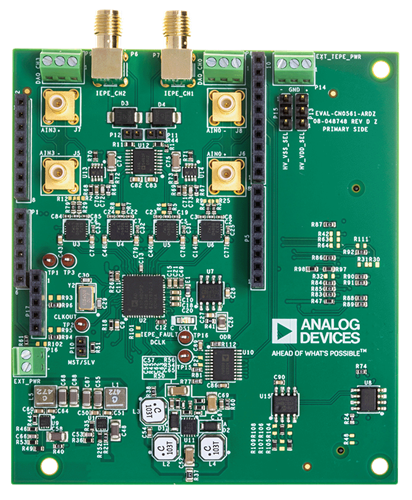
This section outlines the testing procedures and the gathering of the results for the EVAL-CN0561-ARDZ circuit design.
Note that the EVAL-CN0561-ARDZ can interface with 2 different sets of digital hosts either through the arduino headers or using the FMCZ connector.
EQUIPMENT NEEDED
- EVAL-CN0561-ARDZ reference board
- NUCLEO-H563ZI board
- IIO scope Software
USB Type C to USB cable - Precision ac source (for example, AP2700, Brüel & Kjær, or similar precision sine generator)
Getting Started
The basic test setup requires the EVAL-CN0561-ARDZ board to be plugged into the Nucelo-H563ZI board. The Nucleo H563ZI board is required to capture and display the data. Software is available on the https://wiki.analog.com/resources/tools-software/linux-software/iio_oscilloscope.


To test the basic functionality of the board, connect a precision, high quality sine wave or arbitrary waveform generator to the analog input connector of the EVAL-CN0561-ARDZ board.
To set up the EVAL-CN0561-ARDZ and the associated software, use the following steps:
- Mount the EVAL-CN0561-ARDZ evaluation board on the carrier
board (NUCLEO-H563ZI) by plugging it into the arduino headers
as shown in Figure 7.


Figure 7. EVAL-CN0561-ARDZ Mounted on Nucelo-H563ZI Board - Connect the USB-C cable to the Nucelo-H563ZI board and to a USB port of your laptop.
- Connect a 12V power supply to the CN0561-ARDZ P16.
- The connected green LED lights up on the NUCLEO-H563ZI board, next to the USB-C connector.
- Provide the analog input signal using the connectors J6 and J8 on the EVAL-CN0561-ARDZ analog input SMA connectors.
- Open the file explorer and open folder NOD_H563ZI. Copy the file EVAL-CN0561-ARDZ.bin to the above folder. The file in the folder will disappears, and file explorer closes automatically once the file is copied.
- The USB connection creates a COM Port to connect to IIO
Oscilloscope GUI running on windows-os. The COM port assigned
to a device can be seen through the device manager for
Windows OS.


Figure 8. USB COM Port Selection - Open the IIO Oscilloscope Connection and select the COM
port for Nucelo-H563ZI. Choose the COM port and board rate
230400. Click the Refresh button.


Figure 9. Serial Port Settings - IIO Oscilloscope Connection shows the device name. Then, click the Connect button.
- Select the AD4134 from the device name dropdown.


Figure 10. IIO Scope Device Selection - Power-on the sine or arbitrary waveform generator using the
following steps:
- Set the signal type to sine wave.
- Set level to 1V p-p at 1kHz.
- Enable the output.
- Run the IIO Scope software and capture the resulting ADC data and FFT data.
- Go to Capture Window and Press the Enable all button.
- Press the Capture button, observe data in 2 complement form.


Figure 11. Data Output


