MAX16165
推荐用于新设计高度集成的4通道时序控制器和监控器
集成监控功能的小尺寸、宽电压范围时序控制器
- 产品模型
- 2
概述
- 宽工作电压范围:2.7V至16.0V
- 可监控多达5个电压
- 可对多达4个电压进行时序控制
- 逆序关机或同时关机
- 无限菊花链
- 可通过电容调节时序控制延迟
- 可通过电容调节电源良好超时
- 可通过电阻配置电源开启和关闭阈值
- 开漏(MAX16165)/推挽(MAX16166)输出
- 提供POK输出,用于系统微控制器复位
- 双向低电平有效FAULT输入/输出
- 4x5引脚WLP和20L TQFN封装
- 工作温度范围:–40°C至+125°C
MAX16165/MAX16166监控多达五个电压,并对多达四个电压进行时序控制。这些器件在每个电源开启时提供可调延迟,并监控每个电源电压,包括输入电压VDD。
MAX16165/MAX16166采用2.7V至16V电源供电,提供内部稳压器输出(ABP),为内部电路供电,并为任何外部电路额外提供超过1mA的电流。
时序控制由两个输入(ON和低电平有效OFF)使能。ON输入的上升沿启动通道的上电时序,低电平有效OFF输入的下降沿启动关断时序。在上电时序期间,当所有电压达到其最终值时,时序完成输出DONE置为高电平,然后在复位延迟定时器超时后输出电源正常(POK),从而使微控制器(µC)运行。如果任何电压低于其阈值,则复位输出置位,并且所有电压都关闭。当时序控制器启动关断时序时,MAX16165/MAX16166可以对输出进行反向时序控制。
提供开漏(MAX16165)和推挽(MAX16166)输出选项。MAX16165/MAX16166可进行任何数量的菊花链连接,对系统中任何数量的电压进行控制。
MAX16165/MAX16166具有双向低电平有效FAULT输入/输出,在任何故障条件下均置为低电平。只要UVSET输入出现欠压事件,低电平有效FAULT就会保持低电平,并且在所有其他低电平有效FAULT条件下都是单次输出。通过外部信号将低电平有效FAULT拉低就会立即禁用所有输出。MAX16165/MAX16166采用1.63mm x 2.03mm、20引脚晶圆级封装(WLP)和4mm x 4mm、20L TQFN封装。该器件的额定温度范围为-40°C至+125°C。
应用
- FPGA/ASIC电源时序控制
- 工业传感器和电机控制
- 多电源系统中的防闩锁和冲击电流保护
- 网络设备
- 服务器和安保摄像头
- 测试设备
参考资料
数据手册 1
技术文章 1
视频 1

产品选型卡 1
产品选型指南 1
ADI 始终高度重视提供符合最高质量和可靠性水平的产品。我们通过将质量和可靠性检查纳入产品和工艺设计的各个范围以及制造过程来实现这一目标。出货产品的“零缺陷”始终是我们的目标。查看我们的质量和可靠性计划和认证以了解更多信息。
| 产品型号 | 引脚/封装图-中文版 | 文档 | CAD 符号,脚注和 3D模型 |
|---|---|---|---|
| MAX16165ATPH+ | Thin Quad Flatpack, No Leads | ||
| MAX16165ATPH+T | Thin Quad Flatpack, No Leads |
这是最新版本的数据手册
软件资源
找不到您所需的软件或驱动?
申请驱动/软件工具及仿真模型
IBIS 模型 1
评估套件
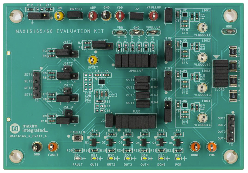
MAX16165/MAX16166评估套件
MAX16165/MAX16166评估套件