The EVAL-LT3078-AZ evaluation board features the LT3078, a 5 A,
ultra-low noise, high power-supply rejection ratio (PSRR), 55 mV
dropout ultra-fast linear regulator. The input voltage (VIN) range
for the VIN power is from 0.6 V to 5.5 V. There are jumpers to
set a 3-bit trilevel code that determines the output voltage (VOUT)
at preprogrammed levels that range from 0.5 V to 4.2 V. The
maximum output current is 5 A. The EVAL-LT3078-AZ requires an
external BIAS voltage (VBIAS) that is at least 1.2 V higher than
VOUT and is between 2.375 V and 5.5 V.
The LT3078 of the EVAL-LT3078-AZ requires few external components,
therefore, simplifying circuit design. External component
choice with careful printed circuit board (PCB) design helps to
optimize noise, PSRR, load-transient response, and VOUT regulation
performance. The LT3078 requires capacitors for the internal
reference, power input, BIASF pin, and the power output. The
internal reference is bypassed with a 16 V, 0805 sized, 4.7 μF
capacitor to reduce output noise and program the soft-start. Larger
capacitor case sizes and higher voltage ratings decrease 1/f noise
for otherwise comparable capacitors. The 10 μF x2 capacitor at the
circuit output was chosen for high-frequency PSRR performance
and to optimize VOUT response during load transients.
The capacitor that bypasses the VIN power for the LT3078 and
the corresponding VIN PCB layout can affect PSRR (for additional
information, see the Best PSRR Performance: PCB Layout for Input
Traces section). The EVAL-LT3078-AZ decouples the VIN power
with a 47 μF capacitor. Less VIN capacitance can improve PSRR
at high frequencies (for the minimum capacitor value required for
VIN, see the LT3078 data sheet). Note that a bulk 220 μF tantalum
polymer capacitor further reduces VIN variation during load
transients and reduces input voltage ringing that can be caused by
inductive input power leads. The PCB has a footprint for an optional
Subminiature Version A (SMA) connector that allows a shielded VIN
power connection to the PCB edge, if required.
The EVAL-LT3078-AZ bypasses the BIASF pin with a 2.2 μF capacitor
instead of the VBIAS supply input. Because the BIASF
pin is isolated from VBIAS by a resistance that is internal to the
LT3078, there is less PSRR degradation when BIASF is bypassed
compared to when VBIAS is bypassed. Otherwise, the effect on
PSRR of the VIN and VBIAS bypass capacitors is similar.
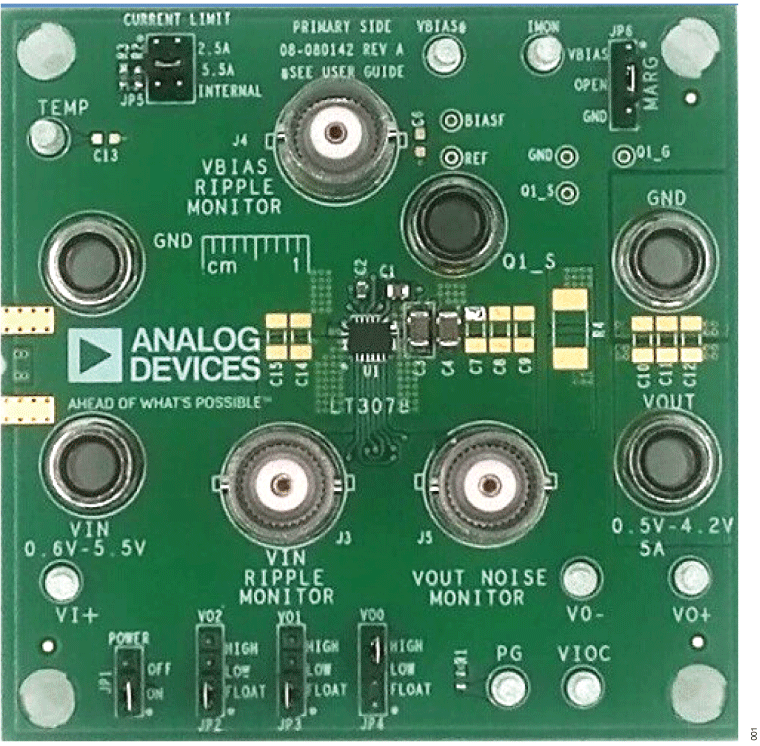
The EVAL-LT3078-AZ has resistors that allow a CURRENT LIMIT
jumper to select output current limits of either 2.5 A or 5.5 A. The
CURRENT LIMIT jumper can also disable external current-limit programming
by shorting the IMON pin to ground. An IMON terminal
is available for current monitoring. The IMON voltage is the product
of the resistance that externally programs current limit and the
IMON pin current that is 1/5000 of the output current. Externally
programmed current limit occurs when the IMON voltage is 1 V.
A POWER jumper (JP1) is available on the EVAL-LT3078-AZ to
either connect the EN pin to VBIAS to turn the output on or to
ground to disable the output. A TEMP terminal is also available
for die temperature monitoring. There is a PG terminal that is
pulled up to VBIAS by a 51 kΩ resistor and pulled down by the
open-drain, negative channel metal-oxide semiconductor (NMOS)
PG pin output for indication of regulator output status and other
fault modes. The voltage input-to-output control (VIOC) terminal
allows connections for automatically controlling a preregulation
voltage. In addition, a MARG jumper can margin the output voltage
to either ±2.5%.
Banana jacks minimize voltage drops on VIN and VOUT connections.
Bayonet Neill-Concelman (BNC) connectors provide low
noise connections to power VIN, VBIAS, and VOUT. The EVALLT3078-
AZ PCB design uses a split-capacitor technique to Kelvin
connect the ground terminal of the REF capacitor to the ground
terminal of the output capacitor, and the SENSE pin to the positive
terminal of the output capacitor. The VO+, VO−, and VI+ terminals
Kelvin connect to VIN and VOUT and are the optimum place to observe
output voltage regulation and dropout voltage performance.
There are test points for BIASF and REF voltages.
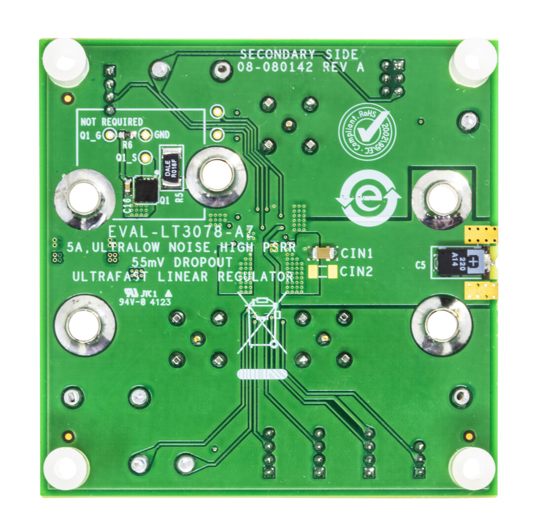
The EVAL-LT3078-AZ includes a load-transient circuit for load response
testing. A 2512 size power resistor must be installed with
a resistance that achieves the required transient current, but all
the remaining circuit components are provided including a 10 kΩ
gate pull-down resistor, a 4.7 nF Miller capacitor and a high-current
NMOS. Additionally, a banana jack makes it possible to return an
external DC load through the same 0.02 Ω sense resistor that is the
return for the transient current so both can be monitored together.
The EVAL-LT3078-AZ has placeholders identified on the schematic
as optional DNI components that make it convenient to add capacitance
(for more information, see Figure 8 in the user guide).
Full specifications on the LT3078 are available in the LT3078 data
sheet available from Analog Devices, Inc., and must be consulted
with this user guide when using the EVAL-LT3078-AZ evaluation
board. The LT3078 of the EVAL-LT3078-AZ features a thermally
enhanced, 22-lead, 3 mm x 4 mm x 0.95 mm LQFN package.
Proper board layout is essential for maximum thermal performance.