ADPA1120
推荐用于新设计4.5W (36.5dBm),8GHz 至 12GHz,GaN 功率放大器
- 产品模型
- 2
概述
- 内部匹配、交流耦合的 4.5W GaN 功率放大器
- 集成式温度补偿 RF 功率检波器
- POUT:在 9.5GHz 至 11.5GHz 频段内,输入功率 PIN = 1dBm 时,典型值为 36.5dBm。
- 小信号增益:典型值 38.5dB,频率范围 9.5GHz 至 11.5GHz
- 功率增益:在 9.5GHz 至 11.5GHz 频率范围内,输入功率 PIN = 1dBm 时,典型值为 35.5dB。
- PAE:在 9.5GHz 至 11.5GHz 频段,输入功率 PIN = 1dBm 时,典型值为 47%。
- 电源电压:20V,50mA,占空比 10%
- 32 引脚,5mm × 5mm,LFCSP
ADPA1120 是一款 8GHz 至 12GHz 的功率放大器,饱和输出功率 (POUT) 为 36.5dBm,功率附加效率 (PAE) 为 47%,在 9.5GHz 至 11.5GHz 范围内,输入功率 (PIN) 为 1dBm 时,典型功率增益为 35.5dB。RF 输入和 RF 输出内部匹配且 AC 耦合。在 VDD1-2、VDD3 和 VDD4 引脚上施加 20V 的漏极偏置电压。通过在 VGG1-2 引脚上施加负电压来设定漏极电流。
ADPA1120 采用氮化镓 (GaN) 工艺制造,封装在 32 引脚、5mm × 5mm 引线框架芯片级封装 (LFCSP) 中,工作温度范围为 -40°C 至 +85°C。
应用
- 气象雷达
- 船用雷达
- 军用雷达
参考资料
数据手册 1
用户手册 1
ADI 始终高度重视提供符合最高质量和可靠性水平的产品。我们通过将质量和可靠性检查纳入产品和工艺设计的各个范围以及制造过程来实现这一目标。出货产品的“零缺陷”始终是我们的目标。查看我们的质量和可靠性计划和认证以了解更多信息。
| 产品型号 | 引脚/封装图-中文版 | 文档 | CAD 符号,脚注和 3D模型 |
|---|---|---|---|
| ADPA1120ACPZN | 32-Lead LFCSP (5mm x 5mm x 0.75mm w/ EP) | ||
| ADPA1120ACPZN-R7 | 32-Lead LFCSP (5mm x 5mm x 0.75mm w/ EP) |
这是最新版本的数据手册
软件资源
找不到您所需的软件或驱动?
申请驱动/软件工具及仿真模型
S-参数 1
评估套件
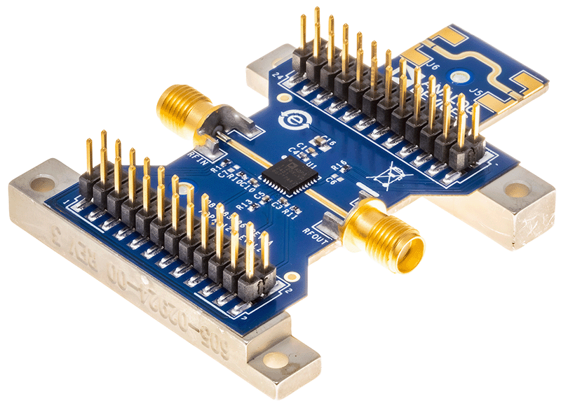
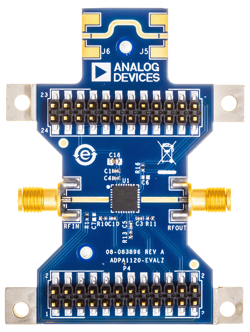
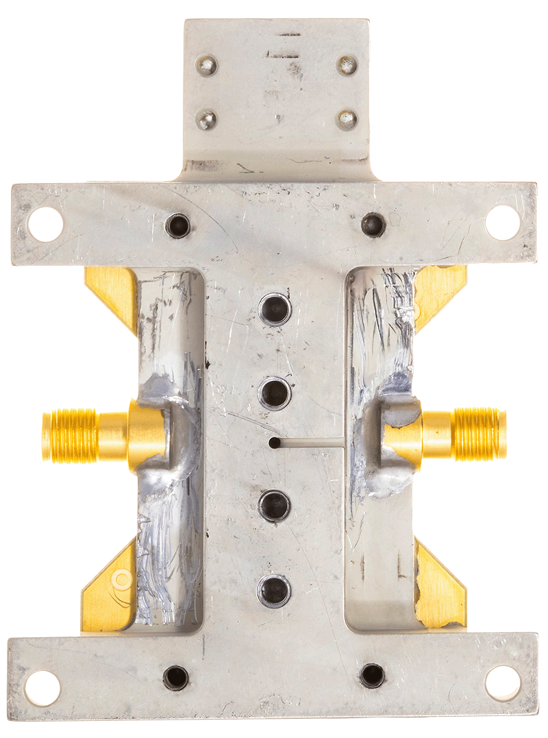
评估 ADPA1120 4.5W (36.5dBm)、8GHz 至 12GHz、GaN 功率放大器
资料
最新评论
需要发起讨论吗? 没有关于 ADPA1120的相关讨论?是否需要发起讨论?
在EngineerZone®上发起讨论