

ADPA9005
推荐用于新设计1GHz to 28GHz, 37.5dBm, GaN Power Amplifier
ADPA9005, 1-28GHz, 37.5dBm PA
- 产品模型
- 2
概述
- Frequency range: 1GHz to 28GHz
- Internally matched and AC-coupled input and output
- Integrated temperature-compensated RF power detector
- Power gain: 9.5dB typical with PIN = 28.0dBm from 6GHz to 25GHz
- POUT: 37.5dBm typical with PIN = 28.0dBm from 6GHz to 25GHz
- Small signal gain: 20.5dB typical from 6GHz to 25GHz
- OIP3: 39.5dBm typical from 6GHz to 25GHz
- VDD: 20V typical
- IDQ: 560mA
- 14-terminal, 7mm × 7mm, LCC_HS package
The ADPA9005 is a 1GHz to 28GHz, wideband power amplifier with a saturated output power (POUT) of 37.5dBm typical, a power-added efficiency (PAE) of 15.5% typical, and a power gain of 9.5dB typical from 6GHz to 25GHz at an input power (PIN) of 28.0dBm. The RF input and RF output are internally matched and AC-coupled. A drain bias voltage (VDD) of 20V typical is applied to the VDD1 and VDD2 pins, which have integrated bias inductors. The drain current is set by applying a negative voltage to the VGG1 pin. A temperature-compensated RF detector is integrated, which allows monitoring of the RFOUT power.
The ADPA9005 is fabricated on a gallium nitride (GaN) process, is housed in a 14-terminal, ceramic, leadless chip carrier with a heatsink, and is specified for operation from −40°C to +85°C.
APPLICATIONS
- Electronic warfare
- Test and measurement equipment
参考资料
数据手册 1
用户手册 1
评估设计文件 1
ADI 始终高度重视提供符合最高质量和可靠性水平的产品。我们通过将质量和可靠性检查纳入产品和工艺设计的各个范围以及制造过程来实现这一目标。出货产品的“零缺陷”始终是我们的目标。查看我们的质量和可靠性计划和认证以了解更多信息。
| 产品型号 | 引脚/封装图-中文版 | 文档 | CAD 符号,脚注和 3D模型 |
|---|---|---|---|
| ADPA9005AEHZ | 14-Terminal LCC_HS (7 mm x 7 mm x 1.063 mm) | ||
| ADPA9005AEHZ-R7 | 14-Terminal LCC_HS (7 mm x 7 mm x 1.063 mm) |
这是最新版本的数据手册
软件资源
EM-Plugs 新
基于EM的RF数字孪生模型
更多内容Evaluation Software 0
找不到您所需的软件或驱动?
工具及仿真模型
S-参数 1
评估套件
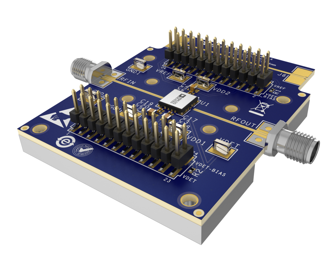
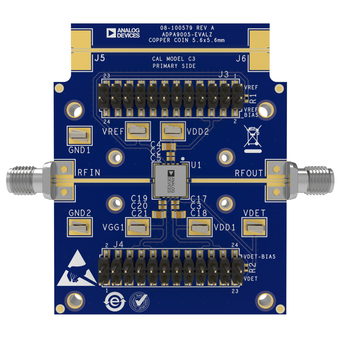
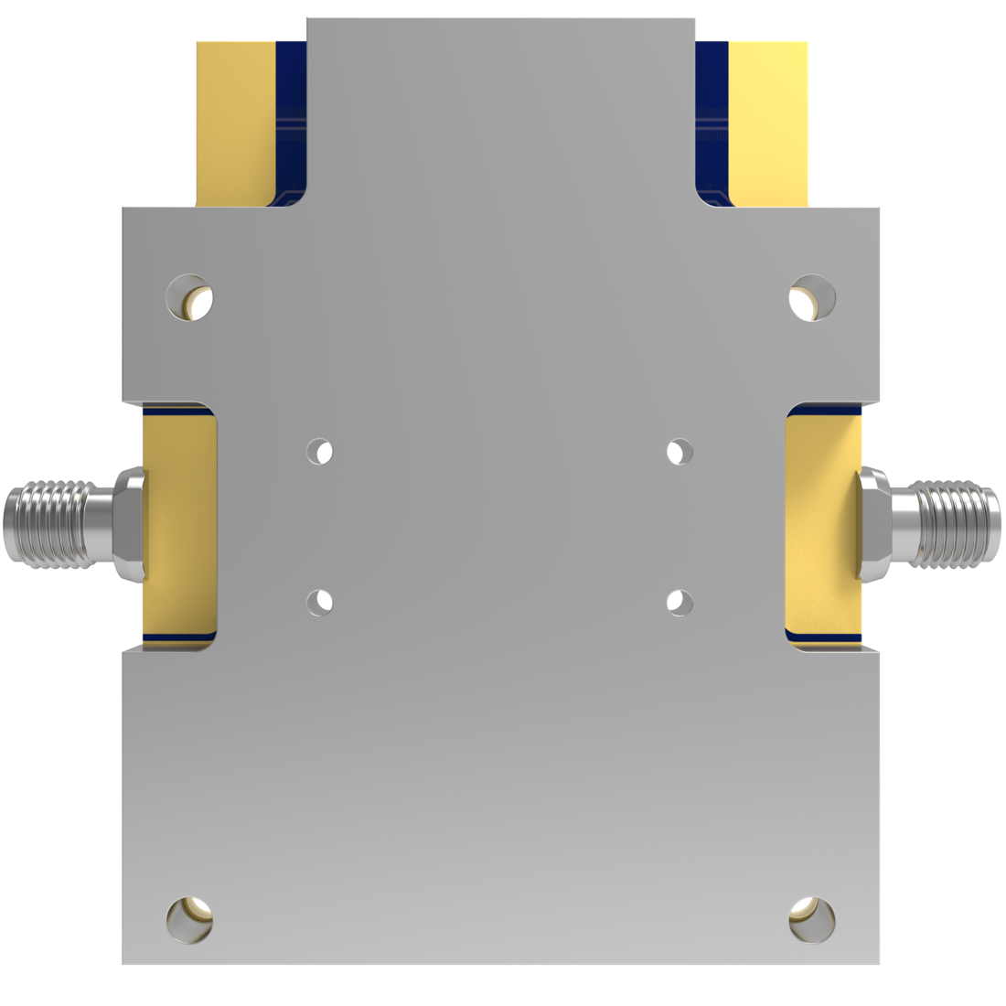
Evaluating the ADPA9005 1GHz to 28GHz, 37.5dBm, GaN Power Amplifier
资料
最新评论
需要发起讨论吗? 没有关于 ADPA9005的相关讨论?是否需要发起讨论?
在EngineerZone®上发起讨论