ADG1712
推荐用于新设计低压、2.4Ω 四路 SPST 开关
- 产品模型
- 1
概述
- ±1.08V 至 ±2.75V 双电源
- +1.08V 至 +5.5V 单电源
- 低导通电阻 2.4Ω
- 16 引脚,2mm × 2mm LGA
- 1.8 V 和 3 V JEDEC 兼容逻辑
- 完全额定电压为±5V、+3.3V、+1.8V 和±2.5V
- 轨到轨信号范围
- 工作温度范围:−40 °C 至 +125 °C
ADG1712 包含四个独立的单刀单掷 (SPST) 开关,采用 +1.08V 至 + 5.5V 的低压单电源范围或 ±1.08V 至 ±2.75V 的低压双电源范围工作。
ADG1712 设计尺寸小巧,但不影响性能。2mm × 2mm 平面网格阵列封装 (LGA) 封装非常适合需要考虑面积的各种应用。
ADG1712 具有仅为 2.4Ω 的低导通电阻和轨到轨输入信号范围。每个开关在打开时在两个方向上的导电性能都一样好。开关通过相应数字控制线上的逻辑 1 输入打开,数字控制输入符合 1.8V 和 3V JEDEC 标准,可轻松与微控制器和现场可编程门阵列 (FPGA) 一起使用。
应用
- 自动测试设备
- 数据采集系统
- 医疗器械
- FPGA 和微控制器系统
- 音频和视频信号路由
- 通信系统
- 继电器替代方案
参考资料
数据手册 1
用户手册 1
ADI 始终高度重视提供符合最高质量和可靠性水平的产品。我们通过将质量和可靠性检查纳入产品和工艺设计的各个范围以及制造过程来实现这一目标。出货产品的“零缺陷”始终是我们的目标。查看我们的质量和可靠性计划和认证以了解更多信息。
| 产品型号 | 引脚/封装图-中文版 | 文档 | CAD 符号,脚注和 3D模型 |
|---|---|---|---|
| ADG1712BCCZ-RL7 | 16-Lead LGA (2 mm x 2 mm x 0.74 mm) |
软件资源
找不到您所需的软件或驱动?
申请驱动/软件硬件生态系统
工具及仿真模型
LTspice
LTspice中提供以下器件型号:
- ADG1712
IBIS 模型 1
LTspice®是一款强大高效的免费仿真软件、原理图采集和波形观测器,为改善模拟电路的仿真提供增强功能和模型。
评估套件
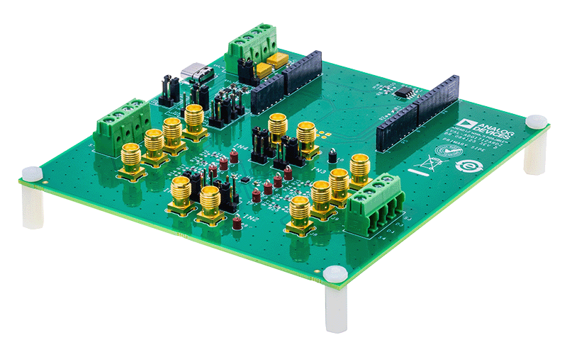
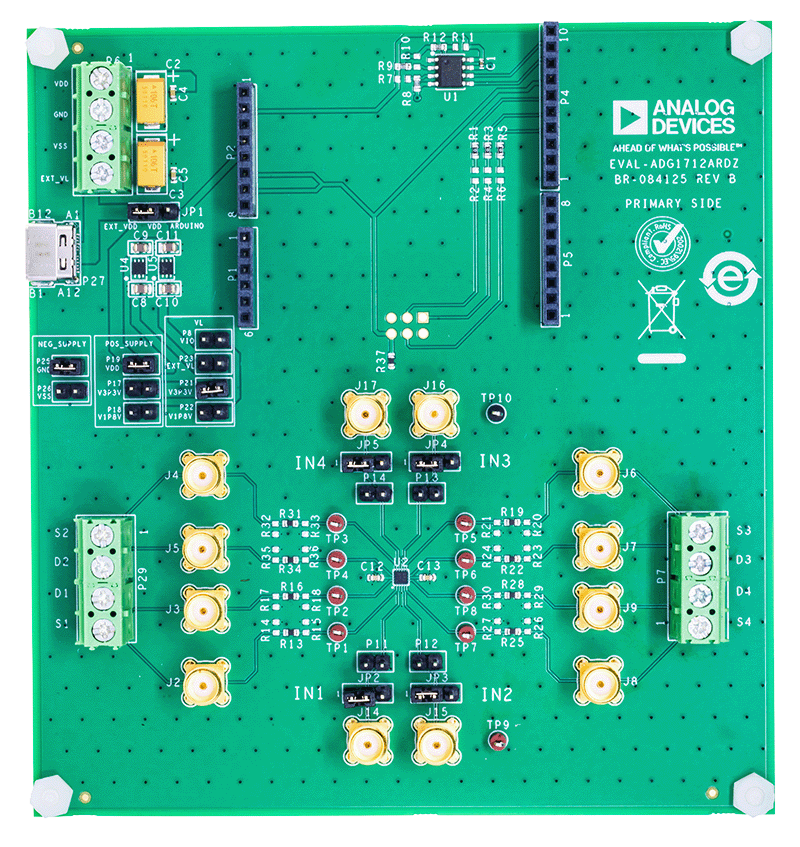
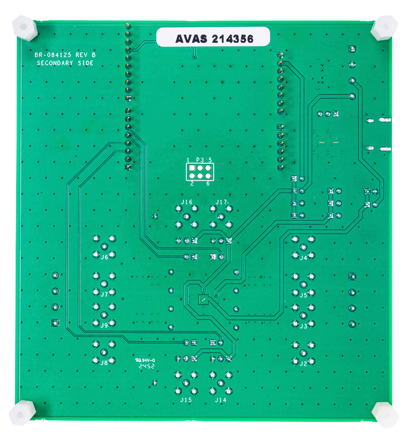
Evaluating the ADG1712, 2.4Ω Quad SPST Switch
资料
最新评论
需要发起讨论吗? 没有关于 ADG1712的相关讨论?是否需要发起讨论?
在EngineerZone®上发起讨论