ADP196
RECOMMENDED FOR NEW DESIGNS5 V, 3 A Logic Controlled High-Side Power Switch
- Part Models
- 4
- 1ku List Price
- Starting From $0.75
Overview
- Low RDSON: 10 mΩ (WLCSP) or 27 mΩ (LFCSP)
- Wide input voltage range: 1.8 V to 5.5 V
- Quick output discharge (QOD) circuit (ADP196-01)
- 3 A continuous operating current at 70°C
- 1.2 V logic compatible enable input
- Low 25 μA quiescent current, VIN 1.8 V
- Low 40 μA quiescent current, VIN = 5.5 V
- Overtemperature and overcurrent protection
- Ultralow shutdown current: <1 μA
- Ultrasmall 1.0 mm × 1.5 mm, 0.5 mm pitch, 6-ball WLCSP
- Tiny 2.0 mm × 2.0 mm × 0.55 mm, 0.65 mm pitch, 6-lead LFCSP
The ADP196 is a high-side load switch designed for operation from 1.8 V to 5.5 V. This load switch provides power domain isolation, helping to extend battery operation. The device contains a low on-resistance, N-channel MOSFET that supports more than 3 A of continuous current and minimizes power loss. In addition, RDSON is constant, independent of the VIN voltage. The low 25 μA quiescent current and ultralow shutdown current make the ADP196 ideal for battery-powered portable equipment. The built-in level shifter for enable logic makes the ADP196 compatible with many processors and GPIO controllers.
Overtemperature protection circuitry is activated if the junction temperature exceeds 125°C, thereby protecting the ADP196 and downstream circuits from potential damage. Overcurrent pro- tection is provided in the form of constant current limiting.
The ADP196-01 incorporates an internal quick output discharge circuit to discharge the output capacitance when the ADP196-01 output is disabled.
The ADP196 in the WLCSP package occupies minimal printed circuit board (PCB) area with a footprint of less than 1.5 mm2 and a height of 0.60 mm.
The ADP196 is available in an ultrasmall, 1.0 mm × 1.5 mm, 0.5 mm pitch, 6-ball WLCSP and a 2.0 mm × 2.0 mm × 0.55 mm, 0.65 mm pitch, 6-lead LFCSP.
APPLICATIONS
- Mobile phones
- Digital cameras and audio devices
- Portable and battery-powered equipment
- In-Rush Control of Optical Network Modules
SFP, SFP+, XFP, CFP
Documentation
Data Sheet 1
User Guide 3
Circuit Note 1
ADI has always placed the highest emphasis on delivering products that meet the maximum levels of quality and reliability. We achieve this by incorporating quality and reliability checks in every scope of product and process design, and in the manufacturing process as well. "Zero defects" for shipped products is always our goal. View our quality and reliability program and certifications for more information.
| Part Model | Pin/Package Drawing | Documentation | CAD Symbols, Footprints, and 3D Models |
|---|---|---|---|
| ADP196ACBZ-01-R7 | 6-Ball WLCSP (1mm x 1.5mm) | ||
| ADP196ACBZ-R7 | 6-Ball WLCSP (1mm x 1.5mm) | ||
| ADP196ACPZN-01-R7 | 6-Lead LFCSP (2mm x 2mm w/ EP) | ||
| ADP196ACPZN-R7 | 6-Lead LFCSP (2mm x 2mm w/ EP) |
| Part Models | Product Lifecycle | PCN |
|---|---|---|
|
Apr 15, 2014 - 14_0080 ADP196 Die Revision |
||
| ADP196ACBZ-01-R7 | PRODUCTION | |
| ADP196ACBZ-R7 | PRODUCTION | |
| ADP196ACPZN-01-R7 | PRODUCTION | |
| ADP196ACPZN-R7 | PRODUCTION | |
|
Aug 8, 2022 - 22_0192 Qualification of an Alternate Adhesive Material and Molding Compound for Select LFCSP Packages |
||
| ADP196ACPZN-01-R7 | PRODUCTION | |
| ADP196ACPZN-R7 | PRODUCTION | |
|
Oct 18, 2016 - 16_0036 Assembly Relocation to Stats ChipPAC Jiangyin and Test Transfer to Stats ChipPAC Singapore of Select LFCSP Products |
||
| ADP196ACPZN-01-R7 | PRODUCTION | |
| ADP196ACPZN-R7 | PRODUCTION | |
|
Aug 6, 2014 - 13_0244 Assembly and Test Transfer of Select 2x2 and 1.6x1.6 mm Mini-LFCSP Products to STATS ChipPAC China |
||
| ADP196ACPZN-01-R7 | PRODUCTION | |
| ADP196ACPZN-R7 | PRODUCTION | |
This is the most up-to-date revision of the Data Sheet.
Software Resources
Can't find the software or driver you need?
Request a Driver/SoftwareEvaluation Kits
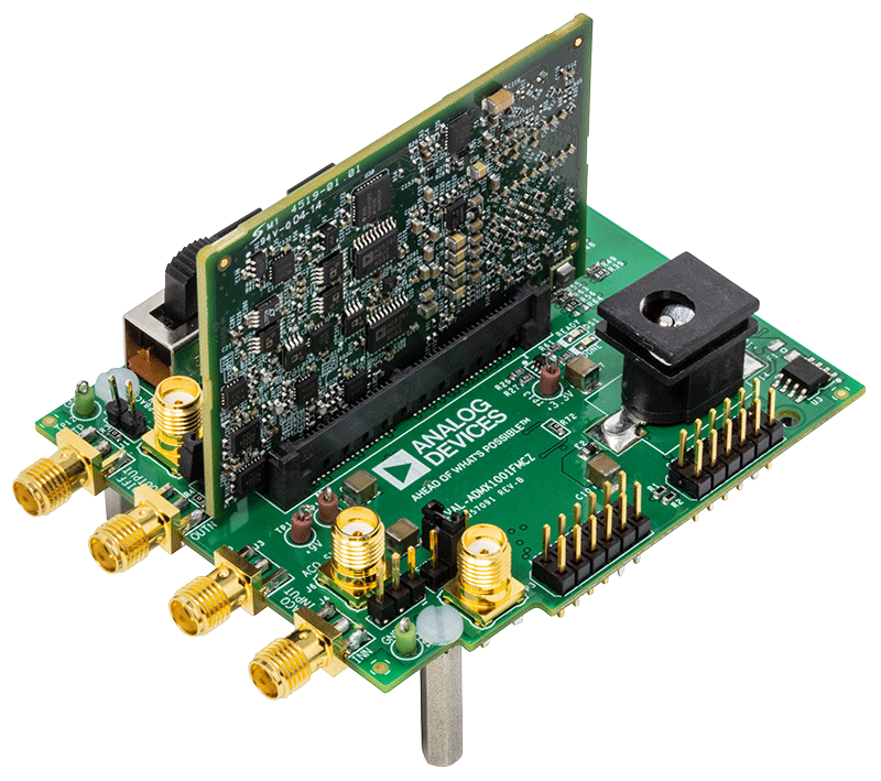
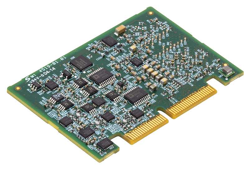
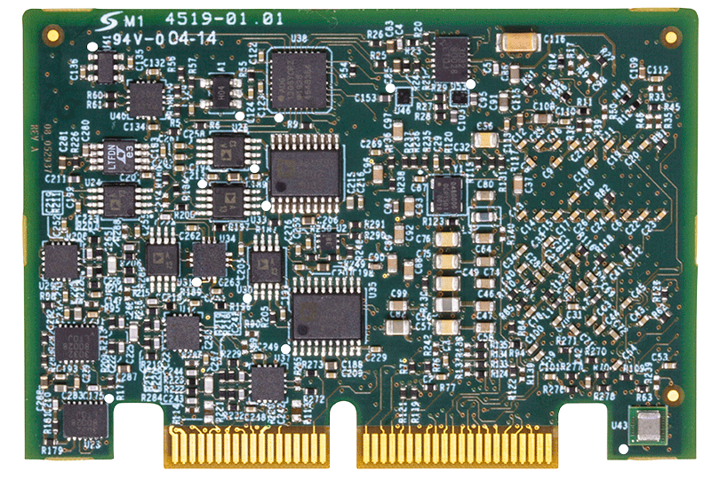
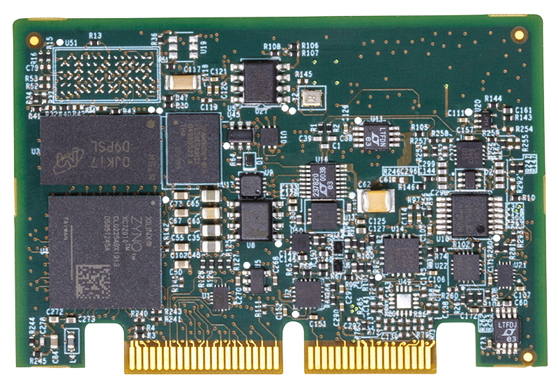
Ultra-low Distortion Signal Generator Measurement Module
Resources
Software
Ultra-low Distortion Signal Generator Measurement Module
Resources
Software


ADP196 Evaluation Board
Resources
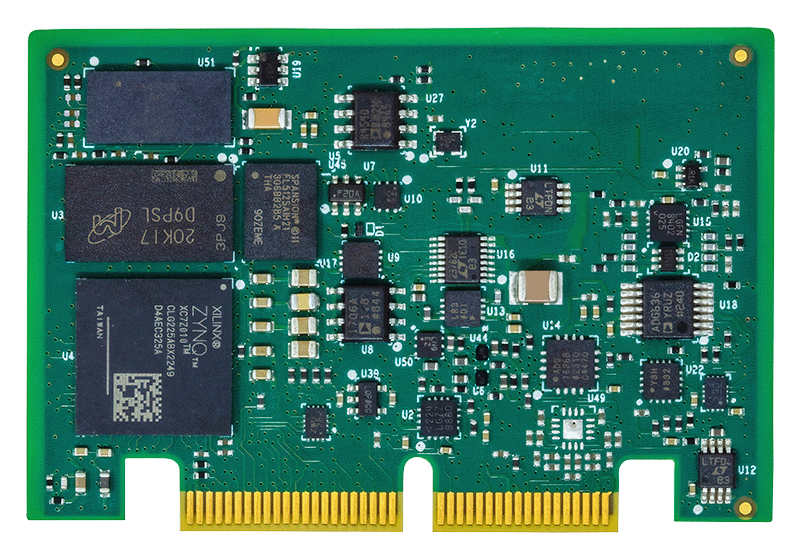
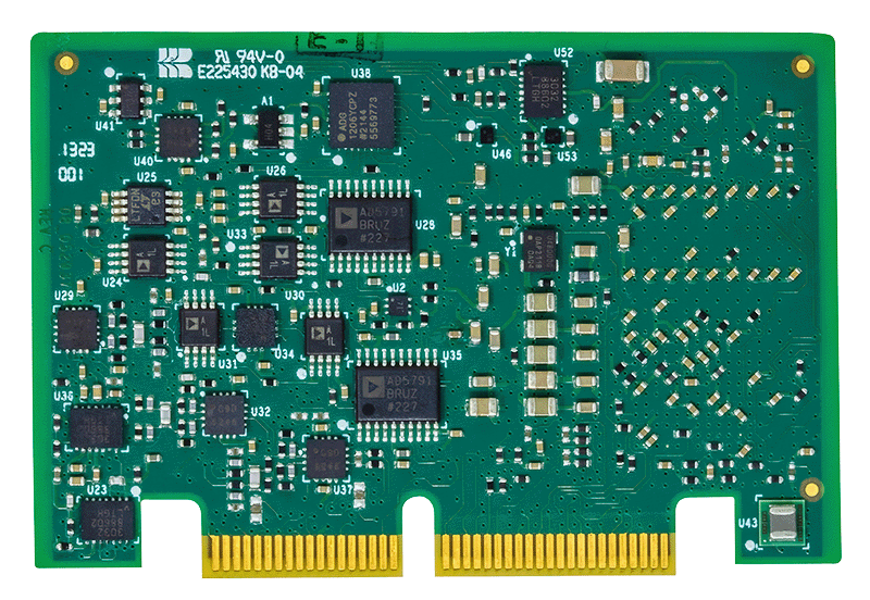
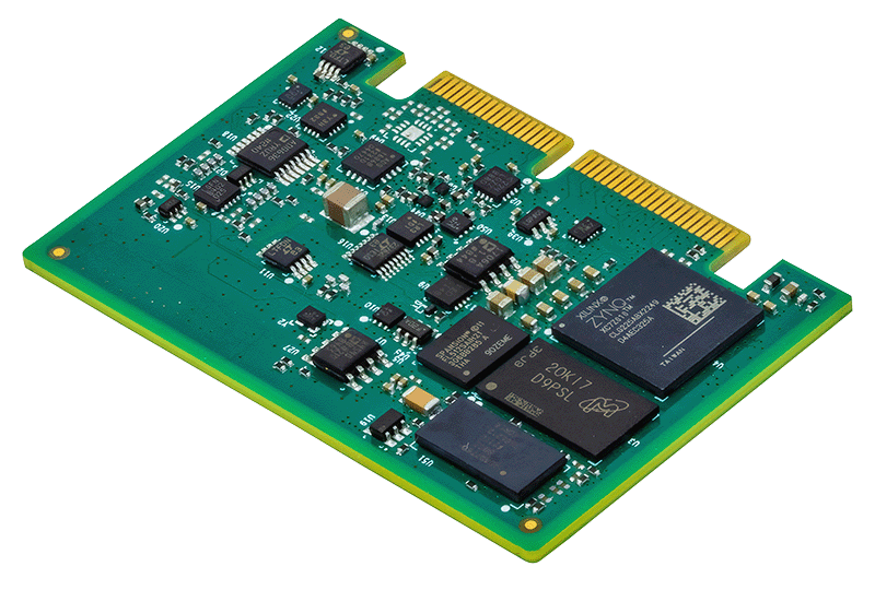
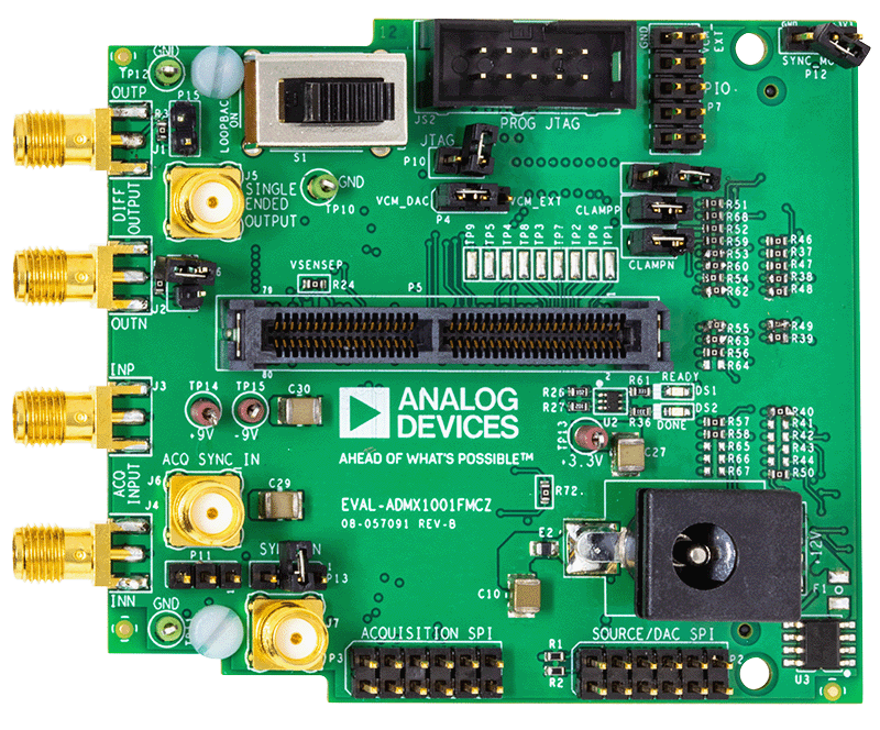
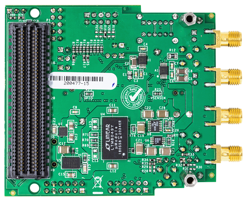
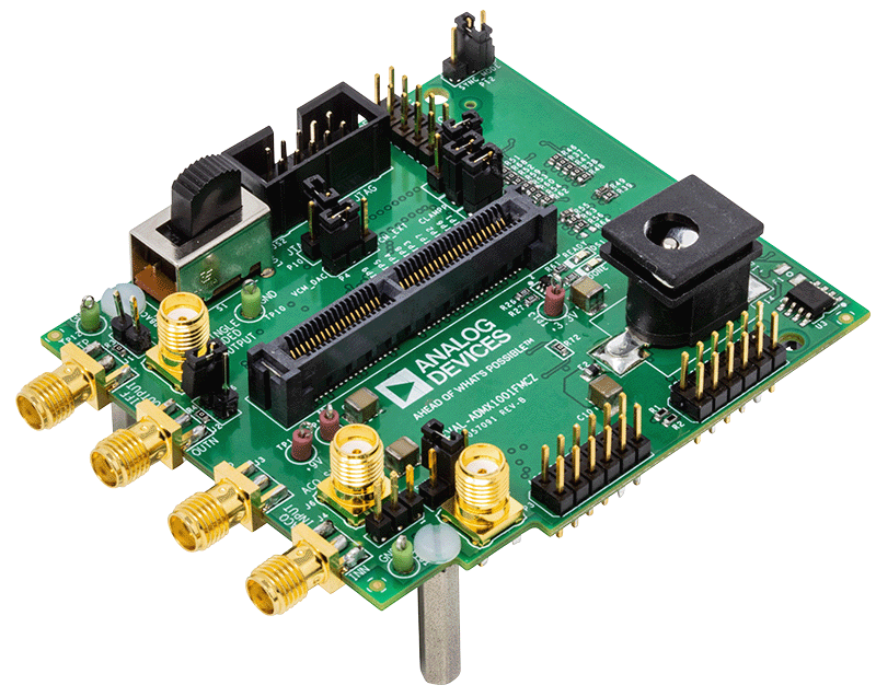
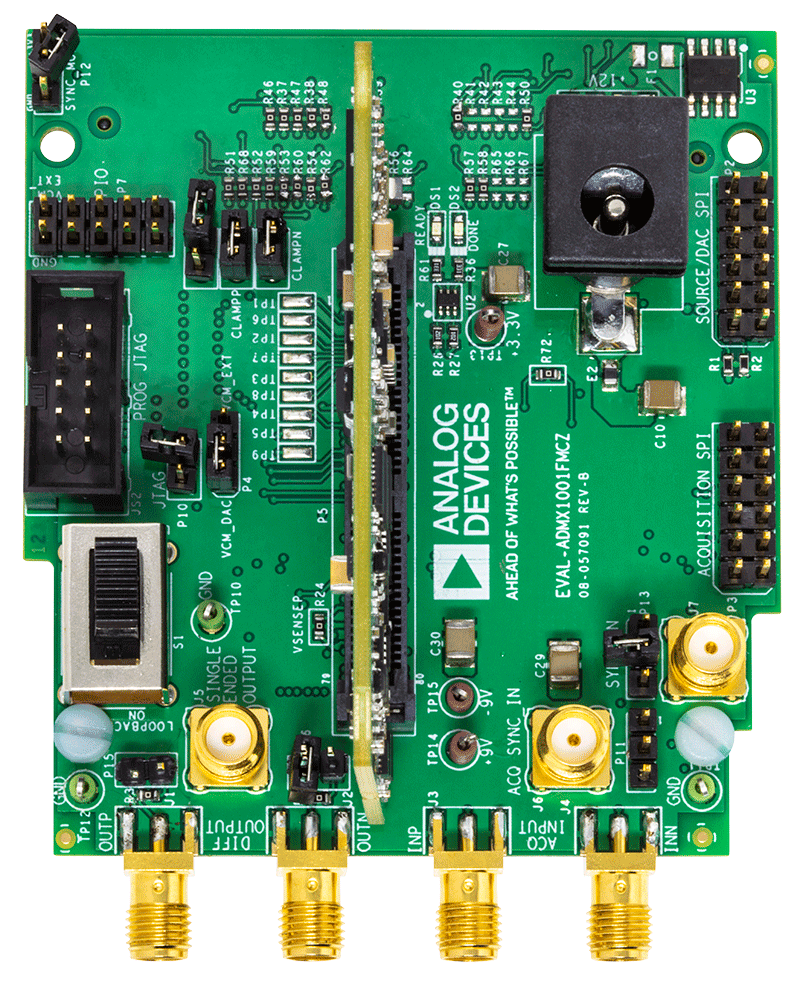
Ultra-low Distortion Signal Generator Measurement Module with Fully Differential Input Acquisition Channel
Resources
Software
Ultra-low Distortion Signal Generator Measurement Module with Fully Differential Input Acquisition Channel