Overview
Design Resources
Design & Integration File
- Schematic
- Bill of Materials
- Gerber Files
- Assembly Drawing
- Allegro Layout Files
Evaluation Hardware
Part Numbers with "Z" indicate RoHS Compliance. Boards checked are needed to evaluate this circuit.
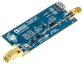
- EVAL-CN0551-EBZ ($45.53) USB-Powered, 433 MHz RF Power Amplifier with Overtemperature Management
Features & Benefits
- +35 dB Gain
- 433 MHz ISM Band Optimized
- 50 Ohm Input and Output Impedance Matched
- Overtemperature Monitoring
- Automatic Thermal Shutoff & Turn on
Documentation & Resources
-
EVAL-CN0551-EBZ User Guide7/15/2022WIKI
Circuit Function & Benefits
The International Telecommunication Union (ITU) allocates the 433.92 MHz industrial, scientific, and medical (ISM) band for use in Region 1, geographically consisting of Europe, Africa, Russia, Mongolia, and the Arabian peninsula. Although originally intended for applications outside radio communications, advancements in wireless technologies and standards over the years have made the ISM band popular for short range, wireless communication systems.
The 433.92 MHz band requires no license for operators in the ITU Region 1 and common applications can be found in software-defined radio, medical equipment, and industrial radio control systems for heavy machinery. In the United States, the 433.92 MHz frequency band is used by licensed amateur radio stations.
In any radio transmission application, a high gain amplifier is required to drive the antenna. This can be implemented in one or more stages depending on the application requirements, with higher output power values extending the range of the RF transmission. To achieve the optimal frequency response, several factors must be considered in the design, such as proper impedance matching, filtering, and thermal management.
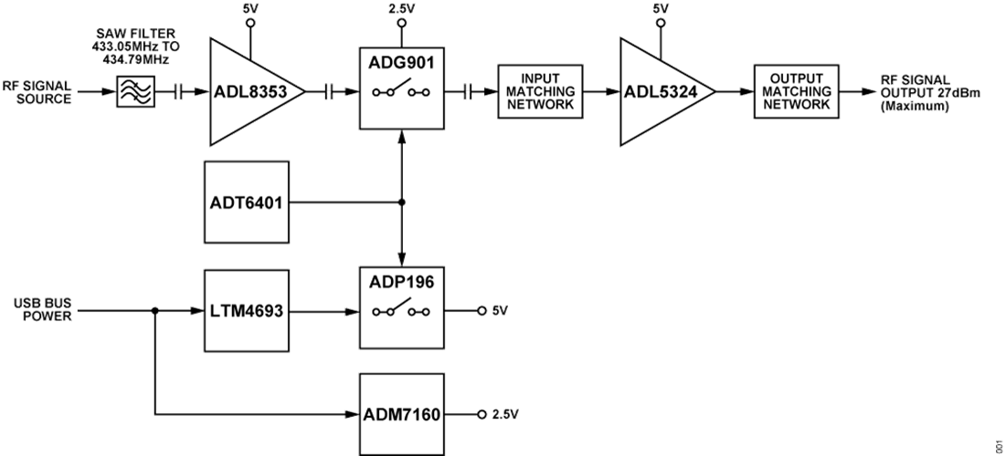
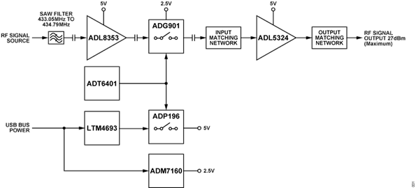
The circuit shown in Figure 1 is a two-stage, RF amplifier block optimized for transmit signal chains operating in the 433.92 MHz ISM band. At the center frequency, the circuit results in a gain of approximately +35.8 dB. The RF input and output ports are designed with a 50 Ω impedance match, enabling direct connection between the circuit and standard 50 Ω systems.
To prevent overheating, a temperature monitoring switch circuit disables the RF amplifier when the user defined temperature trip point is reached. This switch circuitry also automatically enables the amplifier when the temperature falls below the hysteresis set point.
Circuit Description
OPERATING IN THE 433.92 MHZ ISM BAND
The RF signal of the CN0551 is first passed through a surface acoustic wave (SAW) filter before going through the gain stages, which helps eliminate unwanted out-of-band amplification. When selecting a filter, a balance must be struck between the band flatness and the out-of-band rejection. SAW filters are also a source of insertion loss, which reduces the overall gain of the signal chain and needs to be considered during selection.
In this reference design, the SAW filter used has a typical maximum insertion loss of 2 dB and a terminating impedance of 50 Ω.
AMPLIFIER STAGES
The CN0551 uses two amplifier stages in its RF signal path. The first stage is an AD8353 RF gain block amplifier that provides a fixed gain of 19.6 dB (Typical) in the 433.92 MHz ISM band. The AD8353 is capable of operating from 1 MHz to 2.7 GHz, and exhibits a return loss of greater than 10 dB over this entire frequency range.
The RF pins of the AD8353 are internally matched to 50 Ω, allowing it to be integrated directly into standard RF signal paths without external matching networks. As shown in Figure 2, only dc blocking capacitors on the RF pins and bypass capacitors on the supply pins are required for proper operation of the AD8353. Table 1 shows the recommended values for these capacitors.

| Function/Component | Component Values |
| AC Coupling Capacitors | |
| CIN | 1000 pF |
| COUT | 1000 pF |
| Bypass Capacitors | |
| CBYP1 | 100 pF |
| CBYP2 | 0.47 μF |
An ADL5324 RF driver amplifier serves as the second stage of the design. This device has an operating frequency range of 400 MHz to 4 GHz with a typical gain of 18.2 dB, a typical noise figure of 6.8 dB, and a typical output third-order intercept point (OIP3) of 38.4 dBm from 433.05 MHz to 434.79 MHz.
Setting the bias point of the ADL5324 can be done by simply applying +5 V to the RFOUT pin through an RF choke. Using an inductance of 120 nH is recommended because this also provides some of the output matching requirements for the 433.92 MHz ISM band. To filter out RF signals and high frequency noise on the supply lines, the ADL5324 requires three decoupling capacitors on the output stage bias. Figure 3 shows the correct configuration of the bias inductor and capacitors on the RF output stage.

Impedance Matching for the ADL5324
To achieve optimal performance, the ADL5324 requires external matching networks where impedances are tuned for the desired frequency band. The input matching network includes an inductor (LIN) and resistor (RIN) placed in series with the RFIN pin and a shunt capacitor (CIN). Similarly, the output matching network uses a series inductor (LOUT) and a shunt capacitor (COUT). Both the RFIN and RFOUT pins also require external dc blocking capacitors. Figure 4 presents the complete impedance matching network for the ADL5324.

The CN0551 reference design uses similar component values for the 420 MHz to 494 MHz tuning band listed in the ADL5324 data sheet. Refer to Table 2 to see the recommended values.
Proper placement of these components is also critical to the matching; therefore, the CN0551 follows the recommended values for the 420 MHz to 433.92 MHz tuning band in the ADL5324 data sheet.
These values are measured from the center of the component to the edge of the amplifier.
| Function/Component | Component Values |
| AC Coupling Capacitors | |
| CAC1 | 10 pF |
| CAC2 | 20 pF |
| Tuning Capacitors | |
| CIN | 20 pF |
| COUT | 6.2 pF |
| Tuning Inductors | |
| LIN | 1.6 nH |
| LOUT | 5.6 nH |
| Jumper | |
| RIN | 2 Ω |
| Component Spacing | |
| λ1 | 419 mils |
| λ2 | 438 mils |
| λ3 | 248 mils |
| λ4 | 311 mils |
RF PERFORMANCE
The resulting S-parameters, phase noise measurements, and stability measure of the CN0551 are shown in Figure 5, Figure 6, and Figure 7.
At the center frequency of 433.92 MHz, the CN0551 achieves a gain of 35.8 dB. The system exhibits low phase noise with values around -145 dBc/Hz at frequency offsets of 10 kHz and 100 kHz, and -130 dB/Hz at 1 MHz. Values remain below -130 dBc/Hz at frequency offsets above 1 MHz.
The system is stable across the entire 433.92 MHz ISM frequency band with Rollet's stability factor (k) being above 1 and the auxiliary stability measure (B1) being above 0.


Figure 8 shows the output power (POUT) vs. input power (PIN) graph of the CN0551. With the default SAW filter installed on the CN0551, a -3 dBm input results in a maximum ½ W output power. The absolute maximum input power is +10 dBm. It is not recommended to operate the circuit above this input level as damage may incur.

OVERTEMPERATURE MANAGEMENT
An overtemperature management feature is implemented on the CN0551 wherein the amplifier circuitry is automatically disabled when the board temperature reaches a preset threshold. The CN0551 amplifier automatically enables once the temperature falls below the hysteresis set point. This feature is done using the open-drain output (TOVER/TUNDER) of the ADT6401 temperature switch, which monitors the temperature near the ADL5324 and compares it to a pin programmable trip point.
The states of pins S0, S1, and S2 select the temperature trip point and hysteresis of the ADT6401. The available temperature trip point and hysteresis settings on the CN0551 are listed in Table 3.
| S0 | S1 | Temperature Trip Point | Hysteresis |
| 0 | 0 | +65 °C | 10 °C |
| 1 | 0 | +75 °C | 10 °C |
| Float | 0 | +85 °C | 10 °C |
| 0 | 1 | +95 °C | 10 °C |
| 1 | 1 | +105 °C | 10 °C |
| Float | 1 | +115 °C | 10 °C |
| 0 | Float | +5 °C | 2 °C |
| 1 | Float | –5 °C | 2 °C |
| Float | Float | –15 °C | 2 °C |
By default, the CN0551 reference design uses a +95 °C trip point and a +10 °C hysteresis setting.
The ADL5324 has no internal power-down feature that can be directly controlled by the ADT6401 output and so this function has to be implemented externally with switching circuits. In the CN0551, this is done using an ADG901 RF switch and ADP196 power switch to disconnect the RF input and dc bias to the ADL5324. Both of these devices can be turned on or off at the same time using the ADT6401 output, as shown in Figure 9. For the ADG901, a resistor divider with a 1:1 ratio is used to meet the 2.5 V level requirement of the CTRL pin.

For best performance, the thermal resistance of the GND pin of ADT6401 and the GND pin of the heat source needs to be minimized. This is why it is important to place the ADT6401 as close as possible to the ADL5324.
LAYOUT CONSIDERATIONS
The power amplifier produces a large amount of heat when in use; therefore, special attention must be given to the thermal dissipation. To address the power dissipation concerns, the EVAL-CN0551-EBZ uses a 3-layer thick ground plane and multiple thermal vias placed around and under the ADL5324.
Observing the EVAL-CN0551-EBZ using a thermal camera reveals a peak board temperature of approximately 46°C around the ADL5324 with an RF input of -10 dBm, as shown in Figure 10. Combining the thermal dissipation techniques in the layout with the overtemperature monitoring circuitry prevents the ADL5324 from reaching its maximum junction temperature.

USB POWER MANAGEMENT
The CN0551 sources its power via a micro USB port and is regulated to +5 V by an LTM4693 μModule. This ultrathin, standalone, buck-boost DC/DC converter simplifies the regulator circuit design because it already includes a switching mode controller and power devices for a low noise amplifier power supply. The +5 V devices in the CN0551 consume approximately 175 mA during normal operation, mostly drawn by the ADL5324 and AD8353. The two amplifier stages also draw additional supply current at higher temperatures (as described in their respective data sheets). With a maximum continuous output current of 2 A, the LTM4693 is more than sufficient to handle the current requirements of the CN0551.
Proper operation of the LTM4693 only requires a few bypass capacitors, a feedback resistor, and an RC compensation circuit. As shown in Figure 11, CN0551 follows the recommended values in the LTM4693 data sheet for the bypass capacitors and RC compensation circuit. The SS and MODE/SYNC pins are tied to VIN on the CN0551, configuring the device to operate in its low noise,constant frequency pulse-width modulation (PWM) operation with the default 2 ms soft-start period.

The output voltage of the LTM4693 is set by an external feedback resistor (RFB) connected between the VOUT + and FB pins; the value of which is calculated using Equation 1.

where:
VOUT is the desired output voltage in Volts.
RFB is the feedback resistance in kΩ.
For the required output voltage of +5 V, the equation results in an RFB value of 15.1 kΩ. This is implemented in the design as a 15 kΩ resistor.
By default, the LTM4693 has a switching frequency of 1 MHz. However, this can be increased by connecting an external resistor (RT) across the FREQ pin and GND; the value of which is calculated using Equation 2.

where:
fSW is the desired switching frequency in MHz.
RT is the external resistance in kΩ.
Using higher switching frequencies lowers the power efficiency, but this also decreases the output voltage ripple, resulting in a more stable supply voltage for the amplifier. Higher frequencies also help minimize close in phase noise, as shown in Figure 12. For the CN0551, the switching frequency is set to 2 MHz; using this value with Equation 2 results in an RT of 110 kΩ.

The ADM7160 low dropout (LDO) regulator generates the +2.5 V supply voltage required by the ADG901 RF switch. This device has an input voltage range of 2.3 V to 6.5 V and a fixed output voltage that can provide a maximum of 200 mA of current.
To ensure stability of the LDO, high quality capacitors (such as X5R or X7R) that have an effective capacitance (CEFF) greater than 0.7 μF must be used. This also needs to account for the temperature and DC bias effects. Equation 3 can be used to calculate CEFF based on the specifications of the chosen capacitor.

where:
CEFF is the worst-case capacitance in μF.
CBIAS is the effective capacitance at the operating voltage in μF.
TEMPCO is the worst-case capacitor temperature coefficient.
TOL is the worst-case capacitor tolerance.
In CN0551, the capacitors used with the ADM7160 have a rated capacitance of 4.7 μF, a worst-case temperature coefficient of 0.15, and a worst-case tolerance of 0.20. From the capacitance vs. voltage bias graph, the effective capacitance of the input bypass capacitor (+5 V bias) and output bypass capacitor (+2.5 V) is approximately 2.13 μF and 3.60 μF, respectively. Using these values in Equation 3 gives worst-case capacitance values of 1.45 μF and 2.45 μF, both above the minimum requirement of 0.7 μF.
Common Variations
If a power level of 0.5 W is not needed, the ADL5320 can be used as an alternative driver amplifier for the 433.92 MHz ISM band. Compared to the ADL5324, this device offers slightly higher gain and lower noise figure at the cost of having lower OIP3. The saturated output level of the ADL5320 is only around 250 mW.
The ADT6402 can also be used as the temperature switch; this part is pin-compatible and shares the same specifications with the ADT6401, but has an active low output. An inverting buffer is required when using the ADT6402.
Analog Devices also offers similar amplifier designs for transmitting in the 915 MHz and 2.45 GHz ISM bands. For more information, refer to the CN0522 and CN0417 circuit notes.
Circuit Evaluation & Test
This section covers the setup and procedure for testing the S-parameters and phase noise of the CN0551. For complete details, refer to the EVAL-CN0551-EBZ User Guide.
EQUIPMENT NEEDED
The following equipment are used for conducting the tests:
- CN0551 Circuit Evaluation Board (EVAL-CN0551-EBZ)
- Keysight® E5061B vector network analyzer
- Rohde & Schwarz® SMA100A signal generator
- Rohde & Schwarz FSUP signal analyzer
- 20 dB attenuator, which is optional for input protection of the signal analyzer
- 5 V; ≥0.5 A ac/dc power adapter with microUSB cable
- SMA cables
SETUP AND TEST
Figure 13 illustrates the proper port connection of the CN0551 to the vector network analyzer. To measure the S-Parameters, follow below procedure:
- Configure the sweep range and frequency step size of the vector network analyzer. The start and stop frequencies should be set to 433 MHz to 435 MHz, respectively. The frequency step size of the sweep should be set to 10 kHz.
- Perform a full 2-port calibration of the vector network analyzer using a calibration kit. Note that the RF input of the EVAL-CN0551-EBZ can be connected directly to a test port, so only one measurement cable is needed for the test setup.
- Power up the EVAL-CN0551-EBZ using the 5 V power adapter and a micro USB cable.
- Connect the EVAL-CN0551-EBZ across the test ports of the vector network analyzer using the calibrated test setup.
- Set the network analyzer to display the traces of the individual S-parameters.
- Execute the auto scale function on the vector network analyzer. Adjust the scale afterward, if desired.

Figure 14 shows the proper connection of the CN0551 to the signal source analyzer and signal generator for phase noise testing. To measure the phase noise, follow below procedure:
- Set the signal source analyzer to measure phase noise and configure its measurement range. The start and stop offsets should be set to 1 kHz and 30 MHz, respectively.
- Set the signal generator output to a frequency of 433.92 MHz and a level of -10 dBm.
- Refer to the maximum input level on the signal source analyzer data sheet if the equipment can handle the amplifier output (~25.85 dBm at a -10 dBm input). If necessary, connect an attenuator to the input of the signal source analyzer.
- Power up the EVAL-CN0551-EBZ using the 5 V power adapter and micro USB cable.
- Connect the signal generator output to the RF input of the EVAL-CN0551-EBZ.
- Connect the RF output of the EVAL-CN0551-EBZ to the signal source analyzer.
- Start a new measurement run on the signal source analyzer.


