Overview
Design Resources
Design & Integration File
- Schematic
- Bill of Materials
- Gerber Files
- Allegro Layout Files
- Assembly Files
Evaluation Hardware
Part Numbers with "Z" indicate RoHS Compliance. Boards checked are needed to evaluate this circuit.
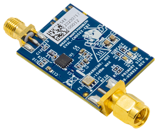
- EVAL-CN0522-EBZ ($47.38) 915 MHz Power Amplifier with Temperature Management System
Features & Benefits
- Optimized for the 915MHz ISM Band
- 1W Power Amplifier
- Overtemperature Management prevents damage to components
Documentation & Resources
-
EVAL-CN0522-EBZ User Guide10/26/2020WIKI
Circuit Function & Benefits
The International Telecommunication Union (ITU) allocates the unlicensed 915 MHz, industrial, scientific and medical (ISM) radio frequency band for use in Region 2, geographically consisting of the Americas, Greenland, and some Eastern Pacific Islands. Within the region, advancements in wireless technologies and standards over the years have made the band popular for short range, wireless communication systems. This ISM band places no restrictions on the application and duty cycle, and common uses include amateur radio, supervisory control and data acquisition (SCADA) systems, and radio-frequency identification (RFID).
Regardless of the application, however, radio transmission in this band requires an amplifier block after the signal chain circuitry to drive an antenna. In the United States, the maximum peak output power for spread spectrum transmitters using the 915 MHz ISM band is either 36 dBm for radio systems using direct sequence spread spectrum (DSSS) or frequency hopping spread spectrum (FHSS) with 50 channels, or 30 dBm using FHSS with less than 50 channels as set by the FCC.
The circuit shown in Figure 1 is a 1 W (30 dBm) RF driver amplifier block optimized for transmitter signal chains operating in the 915 MHz ISM band. At the center frequency, the combination of devices used in this circuit results in a forward gain (S21) and input return loss (S11) of approximately 20 dB and 11.5 dB, respectively. The RF input and output ports of this design are matched to 50 Ω.

Figure 1. CN-0522 Simplified Functional Block Diagram
Circuit Description
Operating in the 915 MHz ISM Band
The RF input signal to the circuit must be passed through a surface acoustic wave (SAW) filter to limit the driver amplifier input to the 902 MHz to 928 MHz frequency band. When selecting a filter, a balance must be struck between the band flatness and the out of band rejection. When considering SAW filters during selection, note that these filters are also a source of insertion loss, which reduces the overall gain of the signal chain.
In this reference design, the SAW filter used has a typical maximum insertion loss of 2.9 dB and a terminating impedance of 50 Ω.
Amplifier
The two-stage RF power amplifier, ADL5605, has an operating frequency range of 700 MHz to 1 GHz with a typical gain of 23.0 dB, a minimum noise figure of 4.7 dB, and a minimum output third-order intercept (IP3) of 43.4 dBm from 881 MHz ±13 MHz.
With the active bias already integrated in the ADL5605, setting the optimal bias points of both amplifier stages can be done by simply applying 5 V on the VBIAS pin and through an RF choke inductor (L1) to the RFOUT pins. It is recommended to use an inductance of 18 nH because this also provides some of the output matching for the 915 MHz ISM band. To filter out RF signals and high frequency noise on the supply lines, the ADL5605 requires three decoupling capacitors on the output stage bias as well as on both of its VCC and VBIAS pins.

Impedance Matching
For the 915 MHz ISM band, the ADL5605 requires no external matching components on its RFIN pin. Meanwhile, matching its RFOUT pins to 50 Ω is done easily by using the microstrip line as an inductor and connecting an additional series inductor (L2) and one shunt capacitor (COUT). External dc blocking capacitors are required on both the RFIN and RFOUT pins.

From the ADL5605 data sheet, the recommended values for L2 and COUT when operating the amplifier at frequencies above 868 MHz are 1.6 nH and 8.0 pF, respectively. Proper placement of these components is critical to the matching. However, simulating the reference design in Keysight’s Advanced Design System (ADS) software results in recommended component spacing values of λ1 = 94.5 mils and λ2 = 240 mils (same as the 925 MHz to 961 MHz band, as seen in the ADL5605 data sheet). These values are measured from the center of the component to the edge of the amplifier.
Small Signal Performance and Phase Noise
The resulting S-parameters and phase noise measurements of the design are shown in Figure 4 and Figure 5. At the center frequency of 915 MHz, the circuit achieves a gain of 20 dB with an input and output return losses greater than 11 dB and 6 dB, respectively. The system exhibits low phase noise with values below −110 dBc/Hz at frequency offsets of 10 kHz and 100 kHz and values are below −130 dBc/Hz and −140 dBc/Hz at frequency offsets of 1 MHz and 10 MHz, respectively.


The output power (POUT) vs. input power (PIN) graph of the design is shown in Figure 6, confirming that the maximum output level of 1 W is achieved at an input level of approximately 11 dBm.

The RF input for this design is limited to the maximum rating of the SAW filter or the amplifier, whichever is lower. With the default on-board SAW filter, the maximum input to the circuit is 15 dBm. The ADL5605 itself can handle an input as high 20 dBm.
Overtemperature Management
An overtemperature management feature is implemented using an ADT6402 temperature switch to monitor the board temperature and disable the amplifier when a set threshold is reached, allowing the EVAL-CN0522-EBZ to cool. With a high accuracy rating of ±0.5°C typical (+6°C maximum, from −45°C to +115°C), the temperature sensor maintains its accuracy and linearity throughout the rated temperature range, eliminating the need for user calibration or correction.

The states of the S0, S1 and S2 pins select the temperature trip point and hysteresis of the ADT6402. On the CN0522, Pin S2 is hardwired to VCC, while Pin S0 and Pin S1 can be connected to either VCC or GND (or kept floating) by using the solder jumpers, JP1 and JP2. These pin configurations limit the temperature trip point and hysteresis options to those listed in Table 1.
| JP1 | JP2 | Temperature Trip Point (°C) | Hysteresis (°C) | ||
| 0 | 0 | +65 | 10 | ||
| 1 | 0 | +75 | 10 | ||
| Float | 0 | +85 | 10 | ||
| 0 | 1 | +95 | 10 | ||
| 1 | 1 | +105 | 10 | ||
| Float | 1 | +115 | 10 | ||
| 0 | Float | +5 | 2 | ||
| 1 | Float | −5 | 2 | ||
| Float | Float | −15 | 2 | ||
| 1 0 is pin tied to GND, 1 is pin tied to VCC, and float is pin left floating. | |||||
Due to the high thermal dissipation of the ADL5605, it is recommended to set the trip point to at least 95°C.
The ADT6402 has an active high, push-pull output (TOVER/TUNDER) that is enabled when the temperature measurement exceeds the trip point. With TOVER/TUNDER connected to the DISABLE pin of the ADL5605 through a buffer gate, the amplifier turns off when the temperature switch trips and only turns back on once the system cools to a temperature below the trip point, plus hysteresis. The buffer gate ensures that the 5 V logic level, 1.4 mA current requirement of the DISABLE pin of the amplifier (ADL5605) is met.
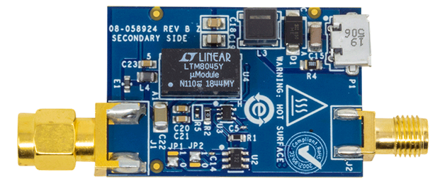
For best performance, the thermal resistance of the GND pin of the ADT6402 and the GND pin of the heat source must be minimized. As such, ADT6402 is mounted on the secondary side of the EVAL-CN0522-EBZ, near the thermal vias connected to the exposed paddle of the ADL5605.
Layout Considerations
Special attention must be given to the thermal dissipation of the circuit as the power amplifier produces a large amount of heat when in use. To ease power dissipation, the EVAL-CN0522-EBZ is designed with a 3-layer thick ground plane and multiple thermal vias placed around and under the ADL5605.
Simulating the CN-0522 design in Cadence® Sigrity™ PowerDC™ software shows that the printed circuit board (PCB) temperature around the amplifier is close to 85°C during normal operation. To achieve a small form factor, no provision for a heat sink was added to the board. Instead, the CN0522 is designed with an overtemperature management feature to maintain the EVAL-CN0522-EBZ temperature at a level where system performance is optimal. This feature also prevents the ADL5605 die from reaching its maximum junction temperature.

USB Power Management Using the LTM8045
Power to the CN0522 is supplied through a microUSB port and regulated by an LTM8045 μModule. This small, standalone dc-to-dc converter simplifies the regulator circuit design because it already includes a current mode controller and power devices for a low noise amplifier power supply.
This design requires approximately 307 mA during normal operation, mostly drawn by the ADL5605 (as the ADT6402 only requires 30 μA). However, note that the ADL5605 draws more supply current at higher output levels. For example, the current draw at a 30 dBm output is >560 mA as described in the ADL5605 data sheet. All active devices used in the CN0522 only require a single 5 V dc supply.
Configured as a single-ended primary conductor (SEPIC), the output voltage of the LTM8045 is set by the value of the feedback resistance (RFB) between the VOUT+ and FB pins and calculated using Equation 1.

where:
RFB is the feedback resistance in kΩ.
VOUT is the desired output voltage in V.
For an output voltage of 5 V, the equation results in an RFB value of 45.3 kΩ, which is implemented in the CN0522 as two resistances of 60.4 kΩ and 182 kΩ connected in parallel to provide two paths for feedback (see Figure 9).

To minimize the noise introduced by the switching transients of the LTM8045, the regulated output is passed through a damped LC filter and a ferrite bead. The filter is designed to suppress switching noise from 80 MHz to 150 MHz. Figure 10 shows an FFT plot of the LTM8045 output noise simulated in LTspice®.

The switching frequency of the LTM8045 is set by an external resistor across the RT pin and GND, and the value of which is calculated using Equation 2.

where:
RT is the external resistance in kΩ.
fOSC is the desired switching frequency in MHz.
For an input and output voltage level of 5 V, the optimal switching frequency for the LTM8045 is 800 kHz as specified in its data sheet. Substituting this value for fOSC in Equation 2, the value of the external resistor is calculated as 115 kΩ. The recommended input and output capacitors for this configuration is 4.7 μF and 100 μF, respectively.

To limit the inrush current from the supply during startup, the LTM8045 is designed to use a soft start function using the external capacitance between SS and GND. To calculate the soft start time, use Equation 3.

where:
tSS is the soft-start time in seconds.
CSS is the external capacitance in μF.
This design uses two 0.1 μF capacitors connected in parallel for the soft start capacitance, resulting in a soft start time of approximately 367 ms.
Common Variations
If a power level of 1 W is not required, the HMC450 can be used as an alternative driver amplifier for the 915 MHz ISM band. Compared to the ADL5605, the HMC450 offers higher gain, noise figure, and input return loss at the cost of having larger output matching requirements and lower output IP3 and output 1 dB compression point (P1dB). The saturated output level of the HMC450 is only around 700 mW.
If the HMC450 is used, the temperature switch must be replaced with the ADT6401, which is pin compatible and shares the same specifications with the ADT6402 but has an active low output.
Analog Devices, Inc., also offers a similar amplifier design for transmitting in the 2.45 GHz ISM band. For more information, refer to Circuit Note CN0417.
Circuit Evaluation & Test
This section covers the setup and procedure for testing the S-parameters and phase noise of the CN0522.
For more information, refer to the CN0522 User Guide.


Equipment Needed
The following equipment is required for conducting testing:
- The EVAL-CN0522-EBZ
- The Keysight® E5061B vector network analyzer
- The Rohde & Schwarz® SMA100A signal generator
- The Rohde & Schwarz FSUP signal source analyzer
- A 5 V ac/dc USB power adapter
- USB Type A to microUSB cable
- SMA cables
- A 20 dB attenuator, which is optional for input protection of the signal source analyzer
Setup and Test
To measure the S-parameters, take the following steps:
- Set the desired measurement conditions of the vector network analyzer. The frequency range must be set such that it includes the 902 MHz to 928 MHz band while the source level must be set to 0 dBm.
- Perform a full 2-port calibration of the vector network analyzer using a calibration kit. Note that the RF input (J1) of the EVAL-CN0522-EBZ can be connected directly to a test port so only one measurement cable is needed for the test setup.
- Power up the EVAL-CN0522-EBZ using the 5 V power adapter and microUSB cable.
- Connect the EVAL-CN0522-EBZ across the test ports of the vector network analyzer using the calibrated test setup.
- Set the measurement to the desired S-parameter.
- Execute the autoscale function on the vector network analyzer. Adjust the scale afterward, if desired.

To measure the phase noise, take the following steps:
- Set the desired measurement configuration of the signal source analyzer.
- Set the signal generator output to a frequency of 915 MHz and a level of 0 dBm.
- Refer to the maximum input level on the signal source analyzer data sheet if the equipment can handle the amplifier output (~20 dBm at a 0 dBm input). If necessary, connect an attenuator to the input of the signal source analyzer.
- Power up the EVAL-CN0522-EBZ using the 5 V power adapter and microUSB cable.
- Connect the signal generator output to the RF input (J1) of the EVAL-CN0522-EBZ.
- Connect the RF output (J2) of the EVAL-CN0522-EBZ to the signal source analyzer.
- Execute a measurement run on the signal source analyzer.


