Power Limitations of Loop-Powered Smart Transmitters
Modern field instruments, otherwise known as smart transmitters, are intelligent microprocessor-based field instruments that monitor process control variables. Such field devices are becoming more intelligent, as some processing capabilities are being distributed into the field domain from centralized control rooms. The incorporation of additional intelligence, functionality, and diagnostic capabilities, while developing a system which can operate effectively within the limited power available from the 4 mA to 20 mA loop is the immediate challenge facing system designers. This article explores the importance of some of the key trends within the marketplace and provides insights into how these can be addressed efficiently at the overall system level and within the fundamental signal chain elements of a smart transmitter design. A sample solution developed by Analog Devices and registered with the HART Communication Foundation [1] focuses on such a design.
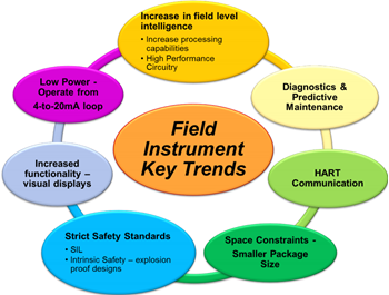
Figure 1. Field Instrument Industry Trends.
The majority of smart transmitters are loop-powered (2-wire) devices. The power taken from the loop must power everything inside the instrument, including the sensor and all supporting electronic circuitry. Since the minimum loop current is 4 mA, the 3.5 mA (“low alarm” setting) maximum allowable system power budget available for such a design, cannot be increased. Hence, power consumption is a primary consideration when selecting components for smart transmitter designs.
Smart transmitters are often located in hazardous or remote areas, and direct access for routine system maintenance tasks is problematic. This is where predictive maintenance functions play a vital role, preventing the need to deploy service personnel into the field. Devices are therefore becoming more self-aware in terms of their own health.
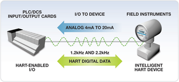
Transmitters communicate process variables to the control room via the standard 4 mA to 20 mA analog loop. This is the preferred communication mode for process critical measurements as it is very robust and is inherently insensitive to noise and voltage drops. With the trend towards the incorporation of more intelligence in the field, HART® (Highway Addressable Remote Transducer) communication is becoming the industrywide 2-way protocol of choice for transmitting additional diagnostics information digitally between the field device and the control room. Simply put, the dc and low frequency 4 mA to 20 mA current signal is modulated by an independent, higher frequency signal that switches between a pair of frequencies (1.2 kHz and 2.2 kHz), a technique known as frequency-shift keying, or FSK. This 1 mA peak-to-peak FSK signal is modulated onto the analog current signal without interrupting the original primary variable transmission.
As with all applications, there is limited PCB area available which leads to restrictions on the type and size of components used. This PCB area restriction is compounded by the combination of transmitter housing size reduction and the need for supplementary functionality. As a result, a high level of on-chip integration is required within each component.
As system level integration becomes more common, the challenge moves towards enhancing the system performance in terms of the accuracy and resolution of its components. Selecting components with specified performance and total error specifications for absolute accuracy and drift over temperature are essential to realize an accurate and stable transmitter solution. This also helps in eliminating the need for multiple costly calibration routines, thus reducing production costs and increasing the manufacturability of the end system.
Having examined some of the key market trends, let’s now take a closer look at an actual loop-powered 4 mA to 20 mA smart transmitter signal chain.
-
The two sensors shown in the signal chain in Figure 3 are common to smart transmitter designs, whereby the primary variable is dependent on a secondary variable, e.g., temperature compensation of a primary variable. The sensing element measures an environmental parameter or process variable. The sensor output signal needs to be conditioned and amplified. A low noise precision instrumentation amplifier is typically used. A key point here is the trade-off between low noise and low power. The conditioned sensor signal is then sampled by an ADC. In order to deliver a high performance 16-bit field instrument output, an ADC with greater than 16-bit resolution is required. A high resolution, high dynamic range sigma-delta ADC is often the architecture of choice. Digital signal processing of the ADC output signal is the next stage in the signal chain. This is done within the microcontroller. A 32-bit RISC controller with >10 MIPS is typically used here, e.g., ARM Cortex™-M3. The controller also needs to be complemented by the appropriate amount of Flash memory, SRAM, and other peripherals such as power-on reset functionality, clock generation, digital interfaces, and a range of diagnostic features. The microcontroller (µC) is thus a complex component, with the potential to require a lot of power, so the more processing that can be done per mW, the better.
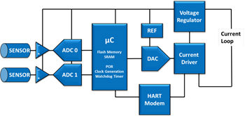
Figure 3. Smart Transmitter Signal Chain.
-
As well as processing the measurements, the μC is used to control the DAC, which, in turn, controls the loop current. Outside of the low power requirement of the DAC, other essential aspects to the selection of this part of the signal chain are high accuracy, temperature stability, and inherent diagnostic capabilities, all of which enhance system performance and stability. The accuracy and stability of the reference supplied to this DAC is also vital.
-
Feeding into the DAC is the HART modem, which, along with the UART interface of the μC, enables HART communication in the smart transmitter design and plays an essential role in retrieving the instrument’s process and diagnostics information. Again, low power and small footprint are important considerations when selecting the HART modem component. The final piece of the puzzle is the power management circuitry, shown in Figure 3, as the voltage regulator block. This takes the power directly from the loop and provides a regulated supply which powers all of the outlined transmitter signal chain components.
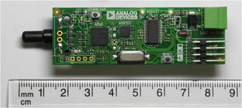
In an application such as this, where every microamp counts, the HART enabled smart transmitter demo circuit (CN-0267) [2] shown in Figure 4 proves invaluable. This circuit, developed by Analog Devices, uses the ADuCM360 [3], a precision analog microcontroller, the AD5421 [4], a 16-bit, 4 mA to 20 mA loop-powered DAC, and the AD5700 [5], a HART compliant IC modem. The analog front-end circuitry is optimized for low power operation while maintaining the required high analog performance. The microcontroller core can be configured in a normal operating mode that consumes 290 μA/MHz. It has very flexible internal power management options, enabling the trade-off of power with a choice of internal clocking speeds and dynamically switching power to the internal blocks. With typical transmit and receive currents of 124 µA and 86 µA respectively, the HART modem will not contribute significantly to the overall current budget. Similarly, the loop-powered DAC has a maximum quiescent current of only 300 µA and a total unadjusted error specification over temperature of ±0.048% FSR, maximizing the granularity of the communicated measurement without adversely affecting system power consumption.
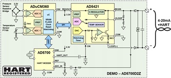
Figure 4. HART Enabled Smart Transmitter Demo Block Diagram.
Examining this solution in more detail, and comparing it to the generic signal chain outlined in Figure 3:
-
The microcontroller on-chip ADC 0 measures the field instrument primary sensor, in this case, a resistive bridge pressure sensor, while the second on-chip ADC is used to measure the secondary temperature sensor signal. This allows for temperature compensation of the primary sensor. Both instrumentation amplifiers are also integrated onto the μC chip, along with excitation current sources, voltage reference, and other support analog circuitry. All the field instrument digital functions are provided by the low power 32-bit ARM Cortex-M3 RISC processor.
-
The second main element in this design is the loop-powered DAC (AD5421), which is interfaced to the μC via the SPI interface. This DAC is a complete, loop-powered, digital to 4mA to 20 mA converter that incorporates the reference, loop interface stage, and the programmable voltage regulation circuitry necessary to extract a low power supply from the loop, to power both itself and the rest of the transmitter signal chain. The DAC also provides a number of on-chip diagnostic features, all of which can be configured and read by the microcontroller, but can also operate autonomously.
-
Finally, the HART modem is connected to the microcontroller via a standard UART interface. The HART output is scaled to the required amplitude by the capacitive divider and coupled to the CIN pin of the DAC, where it is combined with the DAC output, to drive and modulate the output current. The HART input is coupled from LOOP+ via a simple passive RC filter. The RC filter works as the first stage band-pass filter for the HART demodulator and also improves the system electromagnetic immunity, important for robust applications working in harsh industrial environments. The clock for the HART modem is generated by the on-chip low power oscillator with a 3.8664 MHz external crystal with two 8.2 pF capacitors to ground, connected directly to the XTAL pins. This configuration utilizes the least possible power.
Table 1 outlines the breakdown of current in this DEMO-AD5700D2Z system. Not only does it deliver on low power, but it is also a high performance solution, with minimum area overhead, not to mention HART compliance. It has been compliance tested, verified, and registered as an approved HART solution with the HART Communication Foundation. This successful registration provides circuit designers with a high level of confidence when using the components outlined in the circuit.
| Circuit Block | Supply Current (mA) | |
| Sensor | Primary Sensor (Resistive Bridge, 5kΩ at 5V) | 0.660 |
| Secondary Sensor (RTD, 200 μA Excitation) | 0.200 | |
| Total | 0.860 | |
| ADuCM360 | Instrumentation Amplifier 1 (Gain = 8) | 0.130 |
| Instrumentation Amplifier 2 (Gain = 16) | 0.130 | |
| 24-bit ADC 1, Including Input Buffer | 0.140 | |
| 24-bit ADC 2, Including Input Buffer | 0.140 | |
| Voltage Reference, RTD Current Source Reference | 0.135 | |
| uC Core, FLASH, SRAM (Core Clock = 2 MHz) | 0.790 | |
| SPI, UART, Timers, Watchdog, Other Circuitry | 0.085 | |
| Clock Generator | 0.170 | |
| Total | 1.720 | |
| AD5421 | 16-Bit DAC | 0.050 |
| V-to-I Driver | 0.060 | |
| Voltage Reference | 0.050 | |
| Power Management, Voltage Regulators | 0.055 | |
| SPI, Watchdog, Other Circuitry | 0.010 | |
| Total | 0.225 | |
| AD5700 |
Modulator/Demodulator (Worst Case, Transmitting) | 0.124 |
| Clock Generator (with External Crystal) | 0.033 | |
| Total | 0.157 | |
| Other Circuitry on Board, Dynamic Currents, ... | 0.138 | |
| Combined Total | 3.100 |
In conclusion, the circuit outlined above demonstrates one possible solution to the multifaceted challenge involved in the design of a loop-powered smart transmitter to meet ever-increasing market demands. The generic transmitter signal chain discussion, along with the solution offered by Analog Devices, addresses these challenges directly, balancing the allocation of power required by each component, resulting in a comprehensive signal chain addressing the power, performance, size, and diagnostic requirements of a modern, multifeature market-leading smart transmitter design.
