概要
設計リソース
設計/統合ファイル
- Schematic
- Bill of Materials
- Gerber Files
- Assembly Drawing
- Allegro Layout File
評価用ボード
型番に"Z"が付いているものは、RoHS対応製品です。 本回路の評価には以下の評価用ボードが必要です。
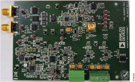
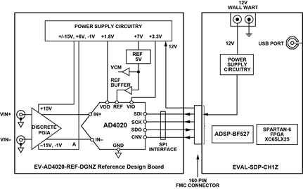
- EV-AD4020-REF-DGNZ ($269.35) 20-bit High Accuracy ADC Reference Design
- EVAL-SDP-CH1Z ($458.85) Evaluation Control Board
デバイス・ドライバ
コンポーネントのデジタル・インターフェースとを介して通信するために使用されるCコードやFPGAコードなどのソフトウェアです。
AD400x PyADI-IIO (Python Interface for IIO Drivers)
FPGA/HDL
機能と利点
- Data acquisition solution fully characterized over 0°C to 70°C
- Guaranteed 20-bit no missing codes
- INL: ±2 ppm, DNL: ±0.25 ppm
- Throughput: 1.8 MSPS
- Offset error drift: ±3.5 ppm/°C; gain error drift: ±6 ppm/°C
- SNR: 98 dB at G = 1, 92 dB at G = 10, fIN = 1 kHz
- THD: −120 dB at G = 1, −116 dB at G = 10, fIN = 1 kHz
- Oversampled dynamic range: 102 dB at 900 kSPS, OSR = 2
- Software programmable bipolar input ranges (±1 V to ±10 V)
- Allows single-ended and differential signals
- CMRR: 92 dB typical
- GΩ input impedance allows direct interface with sensors
- Ease of use features reduce system power and complexity
- ADC Input overvoltage clamp protection sinks up to 50 mA
- On-board 5 V reference and buffer
- First conversion accurate, no latency/pipeline delay
- Fast conversion time allows low SPI clock rates
- SPI-/QSPI-/MICROWIRE-/DSP-compatible serial interface
参考資料
-
UG-1280: EV-AD4020-REF-DGNZ Reference Design Board User Guide2019/05/10PDF1 M
-
シグナル・チェーン・システム用電源ソリューションを簡単に作成する新たな方法2021/12/01
回路説明
System designers developing data acquisition signal chains typically require high input impedance to allow direct interface with a variety of sensors, which could have varying common-mode voltages and unipolar or bipolar single-ended or differential input signals present. The majority of the instrumentation and programmable gain instrumentation amplifiers (PGIAs) are traditionally single-ended output that cannot directly drive a fully differential, high resolution, successive approximation register (SAR) analog-to-digital converter (ADC), and require at least one signal conditioning/driver stage. However, this approach may not always facilitate stringent high accuracy performance, namely, linearity, drift, and speed at desired input levels.
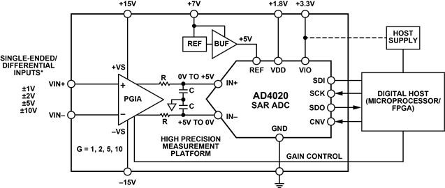
This reference design incorporates the unique discrete PGIA architecture of the Analog Devices, Inc., 20-bit, 1.8 MSPS SAR ADC AD4020, a 5 V reference, and a reference buffer with on-board power supply circuitry. This solution provides a fully characterized, validated design optimized for high precision, offering unprecedented linearity (±2 ppm typical INL), low offset/gain error drift, and trackable noise and distortion (beyond −115 dB) performance at full speed for all gain options over the 0°C to 70°C temperature range. The differential output PGIA uses off-the-shelf discrete components for digitally programmable gains that have GΩ input impedance, over 92 dB common-mode rejection ratio, low output noise, and low distortion, making it suitable for directly interfacing with various sensor types and driving a high throughput, high resolution SAR ADC without compromising performance.
REFERENCE DESIGN SOLUTION
This reference design can resolve either bipolar or unipolar single-ended or fully differential input ranges up to ±10 V with software programmable four gain options (G = 1, 2, 5, and 10). In addition, it allows higher order antialiasing filter and overrange calibration options in PGIA. This solution offers precision ratiometric performance and simplifies system design challenges by eliminating signal buffering/amplification/ attenuation, common-mode level shifting, rejection, settling time, and any other analog signal conditioning challenge allowing for a smaller form factor, faster time to market, and lower cost.
The ease of drive ADC AD4020 incorporates high-Z mode that reduces nonlinear input current, coupled with a long acquisition phase, allowing direct interface to PGIA with a simple RC filter in between. The AD4020 high throughput accurately captures higher frequency signals and allows decimation to achieve wide dynamic range for accurately capturing low level signals, as well as reduces antialiasing filter challenges. The AD4020 consumes only 15 mW at 1.8 MSPS and its power scales linearly with throughput.
The AD4020 serial peripheral interface (SPI) compatible with 1.8 V, 2.5 V, 3 V, and 5 V logic offers user-programmable modes and read/write capability to enable/disable the ease of use features. Note that the features of the reference design differ from that of the AD4020 device itself and, likewise, offer different performance parameters.
| Input Signal (V) | Gain Option |
| Differential | |
| ±1 | G = 5 |
| ±2.5 | G = 2 |
| ±5 | G = 1 |
| Single Ended | |
| ±1 | G = 10 |
| ±2 | G = 5 |
| ±5 | G = 2 |
| ±10 | G = 1 |


