Overview
Design Resources
Design & Integration File
- Schematic
- Layout Files
- Bill of Materials
- Software
- LTspice Simulation Circuit
Evaluation Hardware
Part Numbers with "Z" indicate RoHS Compliance. Boards checked are needed to evaluate this circuit.
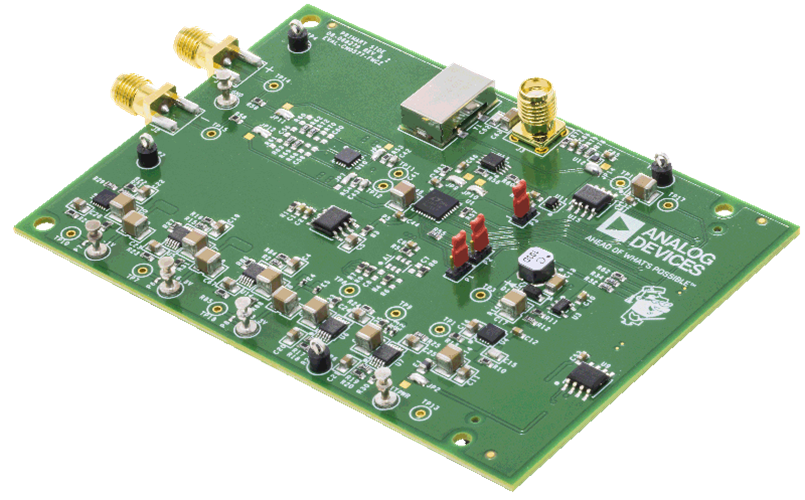
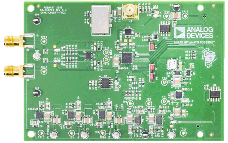
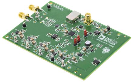
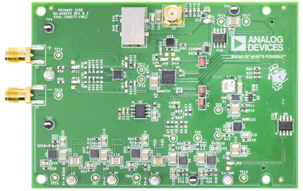
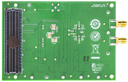
- EVAL-CN0577-FMCZ ($287.50) 18-bit, 15 MSPS, 2 ppm linear Data Acquisition Card
Device Drivers
Software such as C code and/or FPGA code, used to communicate with component's digital interface.
FPGA/HDL
Features & Benefits
- 18-Bit Resolution, 15 MSPS Data Acquisition System
- Arbitrary Voltage Inputs Supported
- All Clocking and Power Requirements are Onboard
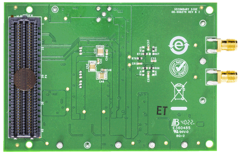
- FMC Connector for FPGA Interfacing
Documentation & Resources
-
EVAL-CN0577-FMCZ User Guide (GitHub)4/16/2026
-
Solutions For Rapid Prototyping: Answering the Needs of Practicing Engineers8/23/2023PDF784 K
Circuit Function & Benefits
Instrumentation applications such as flow cytometry, optical pulse measurement, fast control loops, fast digital distortion correction, and image sensor digitization present unique data acquisition challenges. These applications often require a combination of high sample rate, high linearity, low drift, low noise, and low latency.
Traditional successive approximation register (SAR) analog-to-digital converter (ADC) based digitizers offer low noise performance and low power, but sample rates are typically 2 MSPS or lower. Another strategy is to use a very high speed pipeline ADC and downsample the output. While this technique works in certain applications, pipeline ADCs typically have higher noise and higher drift than SAR ADCs, in addition to having several samples of pipeline delay.
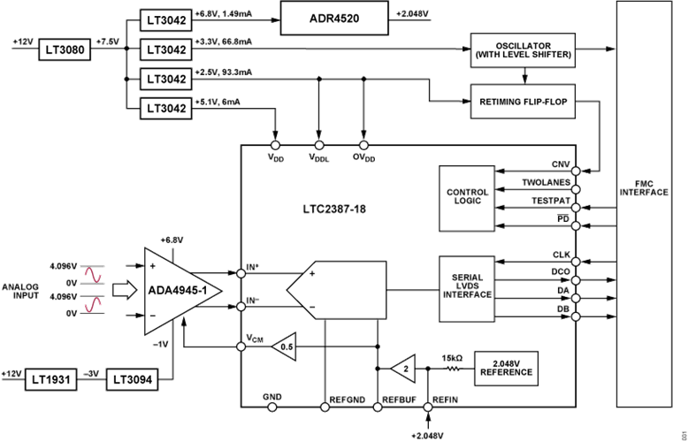
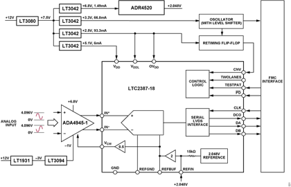
The circuit shown in Figure 1 is an 18-bit, 15 MSPS, 2 ppm linear data acquisition system with an easy to drive input impedance of 1.1 kΩ. The analog input range is 8.096 V peak-to-peak and can be driven in either single-ended or differential mode, providing flexibility for many different applications. Signal-to-noise ratio (SNR) is typically better than 90 dB and total harmonic distortion (THD) is better than -110 dB.
The circuit is in field programmable gate array (FPGA) mezzanine card (FMC) form factor, powered with 12 V either from the FMC connector or an external supply. The digital interface uses serial low voltage differential signaling (LVDS), minimizing the input/output requirements and enabling easy integration with FPGAs.
A separate data clock output eases the timing requirements of the host FPGA. An on-board 120 MHz clock is forwarded to the FPGA and a CONVERT retiming flip-flop reduces jitter from the convert signal of the FPGA.
Circuit Description
ANALOG FRONT END
The most important feature of the CN0577's analog front end (AFE) is to provide an easy to drive input that can be driven arbitrarily (single-ended, differential, or pseudo differential), while meeting the strict drive requirements of the ADC.
The LTC2387-18 SAR ADC requires a fully differential analog input with a common-mode voltage equal to half of the REFBUF voltage, which also sets the input range. The CN0577 sets the REFBUF voltage to 4.096 V, resulting in an input range of ±4.096 V, and a required common-mode voltage of 2.048 V.
The ADA4945-1 is a low noise, low distortion, fully differential amplifier (FDA) that is ideal for driving the LTC2387-18. Offset voltage and drift are 10 μV and 100 nV/°C, respectively; and the input voltage noise is 1.8 nV/√Hz (full power mode, 100 kHz).
The LTC2387-18 includes a VCM output intended to set the input common-mode voltage either through a passive network or by driving a fully differential amplifier's VOCM pin. The VCM output impedance is 15 Ω and can directly drive the 125 kΩ impedance of the ADA4595-1's VOCM pin.
The ADA4945-1 input and output pins are DC-coupled, and the inputs self bias to zero differential voltage when driven through an external AC coupling capacitor. The ADA4595-1 uses supply voltages of +6.8 V and -1 V, maximizing the input range and ensuring that the outputs can utilize the full-scale input range of the ADC.
As shown in Figure 2, the VOCM pin of the ADA4945-1 is connected to the VCM pin of the LTC2387-18, and the output is fully differential.

Input Range and Common-Mode Range
The ADA4945-1 is configured in unity gain, and since the LTC2387-18 input range is fixed at ±4.096 V, this is also the input voltage range of the analog front end. The CN0577 can accept differential, pseudo differential, or arbitrary input signals.
Figure 3 through Figure 6 show CN0577's input signal capabilities in different configurations.


The limitations on the input common-mode are determined by the allowable common-mode range at the ADA4945-1 summing nodes (IN+, IN-), which is specified as -VS to +VS-1.3 V. Arbitrary drive is not easily analyzed, so the end application's worst-case situations should be verified using the LTspice® simulation software.
The LTspice® circuit shown in Figure 7 is configured such that the input’s common-mode (VIN_CM) and differential mode (VIN_NORMAL) can be driven independently, allowing arbitrary signals to be easily simulated. Similarly, the output differential component (VOUT) and common-mode component (VOCM_VERIFY) are verified independently, allowing improper operation to be easily detected.

Figure 8 shows the input common and differential mode, as well as the output.


Figure 9 shows the output common-mode; VCMH and VCML are the upper and lower limits on the LTC2387-18 input common-mode, which VOCM_VERIFY must stay between.
Note the regions in Figure 9 where VOCM_VERIFY exceeds VCMH, and how that corresponds to clipping on VOUT in Figure 8 at the same points in time. This simulation can be accessed in the design support package.
Calculating the Input Impedance
The effective input impedance depends on whether the signal source is single-ended or differential. For a balanced differential input signal as shown in Figure 10, the input impedance between the inputs (+DIN and −DIN) are described in Equation 1:

where:
RIN_DIFF is the differential input impedance.
RG is the gain resistor.

For an unbalanced single-ended input signal as shown in Figure 11, the input impedance can be calculated using Equation 2 to Equation 4:


where:
RIN_SE is the impedance of single-ended input signal.
RG1 and RG2 are the gain resistors.
RF1 and RF2 are the feedback resistors.
β1 and β2 are the feedback factors.

Output Filtering
A filter network must be placed between ADA4945-1's output and LTC2387-18's input to both minimize the noise contribution of the ADA4945-1 and reduce disturbances reflected from the ADC sampling transients. A simple one-pole, low-pass RC filter is sufficient for many applications. It is important that the RC time constant of this filter be small enough to allow the analog inputs to settle within the ADC acquisition time, as insufficient settling can limit integral linearity (INL) and total harmonic distortion (THD) performance.
The value of the filter capacitors involves a trade-off where larger values give lower noise and smaller values gives lower full-scale error. Figure 12 shows a range of capacitor values to consider as a starting point based on sample rate.

The CN0577 uses an 82 pF capacitor (close to the optimal value at 15 MSPS) and a 24.9 Ω resistor, resulting in a cutoff frequency of 77.95 MHz. The filter has minimal impact on noise given the FDA's 1.8 nV/√Hz wideband noise, the ADC's noise density of 17 nV/√Hz, and full power bandwidth of 200 MHz. However, the filter attenuates sampling glitches from the ADC's 18 pF sampling capacitors, ensuring complete settling between samples.
ANALOG-TO-DIGITAL CONVERSION
The LTC2387-18 is a low noise, high speed, 18-bit, 15 MSPS SAR ADC. This device has an exceptional performance with a 2 ppm INL, 96 dB SNR, and -117 dB THD. Applying post-filtering results in a 164 dB dynamic range, normalized to a 1 Hz bandwidth.
The LTC2387-18 operates in two phases. During the acquisition phase, the sample capacitors are connected to the analog input pins IN+ and IN– to sample the differential analog input voltage. A rising edge on the CNV pin initiates a conversion. During the conversion phase, the ADC is sequenced through a successive approximation algorithm, comparing the sampled input with binary-weighted fractions of the reference voltage (e.g., VREFBUF/2, VREFBUF/4 … VREFBUF/262144) using a differential comparator.
The ADC digitizes the full-scale analog input voltage and the control logic prepares the 18-bit digital output code for serial transfer, resulting in an LSB size of 31.25 μV with REFBUF = 4.096 V. The output data is in two’s complement format. The ideal transfer function is shown in Figure 13.

The analog inputs can be modeled using the equivalent circuit shown in Figure 14. The diodes and 10 Ω resistors at the input provide electrostatic discharge (ESD) and overdrive protection. In the acquisition phase, each input sees approximately 18 pF (CSAMPLE) from the sampling capacitor in series with 28 Ω from the on-resistance of the sampling switch. CPAR is a lumped capacitance on the order of 2 pF formed primarily of diode junctions.

Voltage Reference
The LTC2387-18 has a precision internal 2.048 V reference with a guaranteed 0.25% initial accuracy and a ±20 ppm/°C (maximum) temperature coefficient. A 2.048 V, low noise, low drift bandgap reference drives an internal reference buffer with a gain of 2×, producing 4.096 V at REFBUF. The voltage difference between REFBUF and REFGND determines the full-scale input range of the ADC.
The internal reference is adequate for many applications, but an external reference can be used to increase initial accuracy and lower drift. The CN0577 includes an ADR4520, which an ultralow noise, high accuracy 2.048 V voltage reference. This device has an initial accuracy of 0.025% and a drift of 2 ppm/°C. The noise is 1 μVp-p at 0.1 Hz to 10 Hz, and output noise density is 35.8 nV/√Hz at 1 kHz.
The REFBUF amplifier is optimized to drive the fast transient of 0.5 mA to 1.6 mA average load that the ADC presents. The REFBUF voltage is internally divided by 2 to produce a buffered VCM signal that must be used to set the common-mode of the input signal.
DIGITAL INTERFACE
The CN0577 conversion is controlled by the CNV+ and CNV– inputs, which can be driven directly with an LVDS signal. Alternatively, the CNV+ pin can be driven with a 0 V to 2.5 V CMOS signal when CNV– is connected to GND. A rising edge on CNV+ samples the analog inputs and begins the conversion.
After the CN0577 is powered on or exits power-down mode, conversion data is invalid for the first two conversion cycles. The subsequent conversion results are accurate as long as the time between conversions meets the specification indicated in the LTC2387-18 data sheet. If the analog input signal has not completely settled when it is sampled, the CN0577 noise performance is affected by jitter on the rising edge of CNV+. In this case, drive the rising edge of CNV+ with a clean, low jitter signal. Note that the CN0577 is less sensitive to jitter on the falling edge of CNV+. In applications that are insensitive to jitter, CNV can be driven directly from an FPGA.
The CN0577 has an internal clock that is trimmed to achieve a maximum conversion time of 63 ns. With a typical acquisition time of 27.7 ns, throughput performance of 15 MSPS is achieved.
The CN0577 also features a high speed LVDS digital interface with one-lane or two-lane output modes, allowing the user to optimize the interface data rate for each application. Three LVDS pairs are required: CLK±, DCO±, and DA±. A fourth LVDS pair, DB±, is optional, as shown in Figure 15.

Conversion starts at the rising edge of CNV+. When the conversion is complete, the most significant data bit is output on DA±. Data is then ready to be shifted out by applying a burst of nine clock pulses to the CLK± input. The data on DA± is updated by every edge of CLK±. An echoed version of CLK± is output on DCO±. The edges of DA± and DCO± are aligned, so DCO± can be used to latch DA± in the FPGA. The timing of a single conversion is shown in Figure 16.

Data must be clocked out after the current conversion is complete and before the next conversion finishes. The valid time window for clocking out data is shown in Figure 17. Note that it is allowed to be still clocking out data when the next conversion begins.

At high sample rates the required LVDS interface data rate can exceed 400 Mbps, complicating timing constraints. The two-lane output mode cuts the required clock frequency in half. When the two-lane input pin is tied high, the optional LVDS output DB± is enabled; and data is output two bits at a time on DA± and DB±. Enabling the DB± output increases the supply current from OVDD by about 3.6 mA. In two-lane mode, five clock pulses are required for CLK± (see Figure 18).

CLOCK ARCHITECTURE
The CN0577 clock tree is shown in Figure 19. An on-board 120 MHz voltage controlled crystal oscillator is used to provide the clock for the CN0577 and the FPGA. This ultralow noise oscillator has a typical phase noise of -162 dBc/Hz at 10 kHz offset, a tuning voltage range of 0 V to 3.3 V, and a frequency pulling range of 28 ppm to 55 ppm. Additionally, this crystal oscillator has an RMS jitter of <50 fs to 100 fs at 100 MHz carrier.
The clock is fanned out to the retiming flip-flop and the FPGA. An ADG3241 level shifter converts the clock's 3.3 V logic level to the 2.5 V level required by the retiming flip-flop. An ADN4661 converts the 3.3 V clock to LVDS signaling, which is then forwarded to a global clock connection on the FMC connector.

External Clock
If the CN0577 is to be synchronized to other circuits, or if tighter frequency accuracy or drift frequency drift is required, an external clock can be applied to the external clock connector. If the external clock frequency is significantly higher or lower than the on-board 120 MHz clock, reanalyze the entire circuit including the FPGA timing constraints.
The external clock circuitry also includes a high speed single inverter that provides AC coupling and balances the rise and fall times. This device has a typical time propagation delay of 2.4 ns and achieves a high output drive, while maintaining low static power dissipation over a broad VCC operating range.
Retiming Flip-Flop
An FPGA adds jitter to the reference clock. Often the amount of additive jitter is unspecified or unknown, and can significantly reduce SNR. The CN0577 includes a positive-edge-triggered D-type flipflop that provides a low jitter, retimed CNV edge to the LTC2387-18.
This device operates at a supply voltage from 1.65 V to 5.5 V VCC, and has a minimum setup and hold times of 1.7 ns and 0.3 ns, respectively.
To start a conversion, the FPGA provides a high level to the flipflop’s CLR pin. The rising edge of this signal may have significant jitter. The next rising edge of the reference clock propagates a logic high from the flip-flop’s D input to Q output, providing a low jitter CNV edge to the LTC2387-18.
POWER TREE
The CN0577 sources power through the 12 V supply pin of the FMC connector from the FPGA. The power tree was designed using the LTpowerPlanner™, a system-level power architecture design tool. Figure 20 shows the detailed power architecture of this board.
The 12 V supply for this board is first reduced by a pre-regulator stage, an LT3080, an adjustable 1.1 A single resistor low dropout (LDO) regulator. This stage reduces the 12 V supply to 7.5 V, spreading dissipation across the board. This voltage is fed onto the four LT3042 LDOs to generate the 6.8 V, 5.1 V, 3.3 V, and 2.5 V rails.
The LT1931, a 1.2 MHz inverting DC-DC converter, produces a -3 V rail that is fed to an LT3094 low dropout negative regulator to produce a -1 V rail.
The total power consumption of the board is approximately 2.25 W at 15 MSPS.
LAYOUT CONSIDERATIONS
The printed circuit board (PCB) layout is critical to preserve signal integrity and achieve optimum performance. It is recommended to have a multilayer board with an internal, clean ground plane in the first layer beneath the LTC2387-18. Individual components and routing of various signals on the board must also be placed carefully. Additionally, it is recommended to route input and output signals symmetrically.
Ground pins of the ADC must be soldered directly to the ground plane of the PCB using multiple vias. Moreover, ground and power planes beneath the input and output pins of ADC must be removed to avoid undesired parasitic capacitance. Any undesired parasitic capacitance could impact the distortion and linearity performance of the board. The sensitive analog and digital sections are separated on the PCB, while keeping the power supply circuitry away from the analog signal path.
Fast switching signals, such as CNV± or CLK±, and digital outputs DA± and DB± must not run near or cross over the analog signal paths to prevent noise coupling to the ADC.
The LVDS signals should be routed on PCB as 100 Ω differential transmission lines and terminated at the receiver with 100 Ω resistors. Likewise, the fully differential amplifier and voltage reference used in this board require that length of output traces are minimized to avoid parasitic effects. Providing symmetrical layout for complimentary signals ensure maximized and balanced performance of these devices.
High quality ceramic bypass capacitors of at least 4.7 μF must also be added at the output of the on-board LT3042 and LT3094 LDOs to maintain the devices' power supply rejection ratio.
Figure 21 shows the PCB layout of the CN0577 in the vicinity of the LTC2387-18 and ADA4945-1.

Common Variations
The LTC2387-16 is a low noise, high speed, 16-bit 15 MSPS SAR ADC and is pin-compatible with the LTC2387 SAR family. This can be used instead of the LTC2387-18 ADC in this reference design when the intended application only requires 16-bit resolution.
The ADAQ23878 is a μModule® data acquisition solution that provides similar functionality to the LTC2387-18 and ADA4945-1. The digital interface is also compatible.
If more accuracy and/or lower drift is desired, REFIN can be directly overdriven by an external 2.048 V reference. The LTC6655 (2.048 V) is well suited for use with the LTC2387-18 when overdriving the internal reference. The LTC6655 offers 0.025% (max) initial accuracy and 2 ppm/°C (max) temperature coefficient for high precision applications. Bypassing the LTC6655 with a 2.7 μF to 10 μF ceramic capacitor close to the REFIN pin is recommended.
Circuit Evaluation & Test
This section outlines the general setup for evaluating the EVALCN0577-FMCZ. For a complete procedure on the hardware and software setup, refer to the CN0577 User Guide.
EQUIPMENT NEEDED
- EVAL-CN0577-FMCZ
- ZedBoard (AES-Z7EV-7Z020-G)
- 12 V power supply
- Host PC
- MicroSD card (16 GB or larger)
- Analog Devices, Inc. Kuiper Linux image
- LAN cable
- SMA cable
- XLR to SMA adapter cable
- Audio analyzer (Audio Precision© APX525)
- Precision dc source/calibrator (Krohn-Hite 523 or similar)
GETTING STARTED
Recreate the following steps to set up the design for evaluation:
- Download and install the IIO oscilloscope application on the PC, Mac, or Linux host.
- Load the Analog Devices Kuiper Linux image onto the microSD card.
- Configure the microSD card for the EVAL-CN0577-FMCZ.
- Place the microSD card into the ZedBoard.
- Connect EVAL-CN0577-FMCZ to the ZedBoard through the FMC pin connector.
- Connect the 12 V power supply jack on the ZedBoard.
- Plug in the LAN cable from the ZedBoard to the host computer.
- Connect the EVAL-CN0577-FMCZ to the audio analyzer using the XLR to SMA adapter cable.
- Connect the ground of the EVAL-CN0577-FMCZ to the audio analyzer.
- Connect the audio analyzer USB cable to PC.
- Run the IIO oscilloscope software and capture the resulting ADC data and FFT data.
TEST RESULTS
Fast Fourier Transform (FFT) techniques are used to test the ADC’s frequency response, distortion, and noise at the rated throughput. By applying a low distortion sine wave and analyzing the digital output using an FFT algorithm, the ADC’s spectral content can be examined for frequencies outside the fundamental. The LTC2387-18 provides guaranteed tested limits for both AC distortion and noise measurements. Figure 22 shows the FFT performance of the CN0577.

Figure 23 shows the proper connection of the EVAL-CN0577-FMCZ to the audio analyzer for SNR, THD, and SFDR testing.

At 40 kHz differential input signal, with an amplitude of 4.096 Vp-p sitting at a common-mode voltage of 2.048 V and ADC sampling at a rate of 15 MSPS; the measured lowest average SNR and THD is 82.6 dB and -84 dB, respectively. Figure 24 shows the typical performance of CN0577 at different sampling rates and frequency input signal.

Figure 25 presents the proper connection of the EVAL-CN0577-FMCZ to the precision DC source for noise testing.

Figure 26 illustrates the typical DC histogram of CN0577, with REFIN equal to 2.048 V and a sample frequency of 15 MSPS.

Figure 27 presents the error between the ideal voltage and the corresponding voltage input for two different sampling rates, 5 MSPS and 15 MSPS.

