EM-Plugs
製品概要
機能と利点
EMプラグの各モデルは、高周波数設計のためにRF ICの動作を基板、レイアウト、遷移領域の全体にわたってキャプチャする、EMベースのRFデジタル・ツインです。これらのモデルは、手軽に使用でき、かつモジュール化可能であり、正確なEMレベルのモデリング機能を保持しています。
- これが重要である理由:基板およびレイアウトに応じてマッチングと帯域幅が変化しますが、これらの変化の影響はSパラメータのみを使用した場合にはキャプチャできません。
- ブラインド・スポット:Sパラメータはリファレンス・プレーンをチップ境界または50Ωパターンに置き、基板依存および遷移領域依存の挙動にはリファレンス・プレーンを置きません。
- 相違点:EMプラグの各モデルは、遷移領域の挙動をシミュレーションに取り入れているため、「試行錯誤」ベースのテストPCB手法が不要になります。
- CADツールのサポート:EMプラグの各モデルはANSYS HFSS用に提供されています。モデルは暗号化されていないため、必要に応じて他の3D EMソルバにインポートできます。
リストされている互換製品の最新更新日は2026年5月7日です。
*互換製品
- ADTR1101
- ADTR1104
- ADPA7008
- ADPA7006
- ADPA7005
- ADPA1112
- ADPA1106
- ADL8106
- ADL8102
- ADL8108
- ADRF5740
- ADRF5720
- ADRF5721
- ADRF5730
- ADRF5731
- ADRF5476
- ADRF5700
- ADRF5714
- ADRF5715
- ADRF5716
- ADRF5717
- ADRF5030
- ADRF5031
- ADRF5044
- ADRF5045
- ADRF5048
- ADRF5049
- ADRF5420
- ADRF5440
- ADRF5026
- ADRF5027
- ADRF5424
- ADRF5050
- ADRF5051
- ADRF5080
- ADRF5022
- ADRF5023
- ADRF5020
- ADRF5021
- HMC797APM5E
- HMC994APM5E
EMプラグとは?どのように機能するのか?
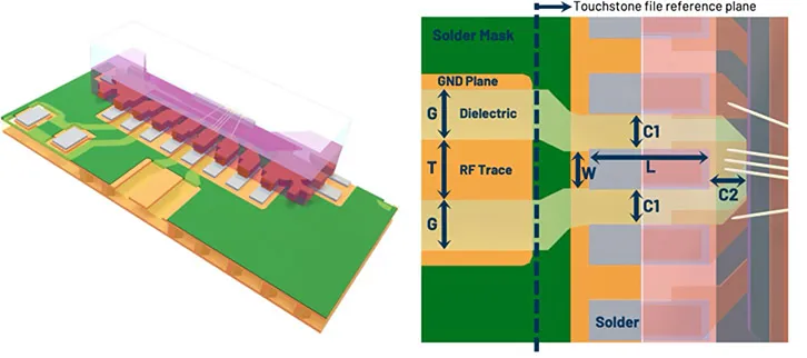
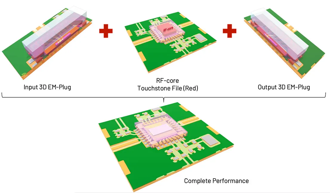
EMプラグ・モデルは、内部リファレンス・プレーンでEMモデル化されたインターフェースから本質的なRFコアを切り離しています。EMプラグ・モデルの3D EMシミュレーションとRFコアを合わせることにより、レイアウトの完全な挙動が表せます。
- RFコア:本質的/コアなRF IC挙動
- EMプラグ:遷移領域(レイアウト)を含むチップから基板までのインターフェースEMモデル。
- 結合モデル:入力EMプラグ + RFコア + EMプラグ = 完全なRF挙動
複数の統合スタイルにわたるパッケージと遷移領域の例
EMプラグ・モデルで可能になること
- PCBの試行錯誤が不要:テスト・ボードやテスト・フィクスチャを構築せずにマッチングと遷移領域の最適化ができるため、初回で成功する確率が向上。
- 手軽で実用的なシミュレーション:フルチップの暗号化されたEMモデルに比べ、はるかに高速(数分~数時間)かつ反復試行が容易。
EMプラグ

- チップからPCB遷移領域まで
- シミュレーションおよび測定ベース
- 全体の設計時間を高速化
- IP制限なし
- ツール無依存
- 重い計算は不要
フル・ウェーブEMモデル

- チップとPCB遷移領域のすべて
- シミュレーション・ベース
- 長いシミュレーション時間
- IPを含め暗号化が必要
- 暗号化によりツール無依存
- 重い計算が必要
マトリックス・ボード

- PCB遷移領域はブラック・ボックス
- 測定ベース
- 製造時間
- IP制限なし
- PCBツールの専門知識が必要
- 製造コスト
EMプラグ・モデル、フル・ウェーブEMモデル、マトリックス・ボードの比較(ワークフローの比較)
- モジュール式設計の詳細:複数の遷移領域やPCB層構成を解析できます。
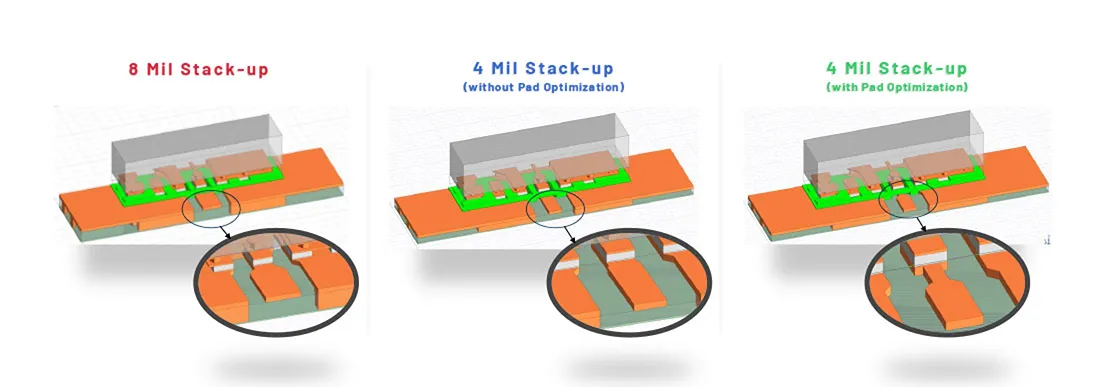
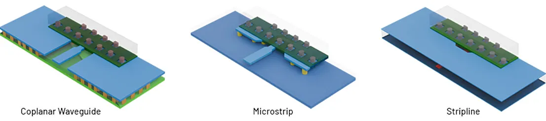
- 重要な変数をすべてキャプチャ:ランド・パターン、層構成(厚さ/εr)、コプレーナ/マイクロストリップ/ストリップライン、ハンダ/マスク、配置/ボンディングワイヤ
早期に実装感度を評価し最適化するには、EM掃引を使用してください。
資料
-
EM-Plugs for RF ICs : Practical EM Models for Fast and Accurate RF Design2026/04/19PDFundefined