ADRV9032R
新規設計に推奨デュアル・オブザベーション・パスを備えた、2T2RのTDDおよびFDDの集積化RadioVerseトランシーバ
- 製品モデル
- 2
- 1Ku当たりの価格
- 価格は未定
製品情報
- 差動トランスミッタ × 2
- 差動レシーバ × 2
- 差動オブザベーション・レシーバ × 2
- LO調整可能範囲:450 MHz~7125 MHz
- RF範囲:350 MHz~7225 MHz1
- トランスミッタの大信号最大帯域幅:200 MHz
- トランスミッタの最大シンセシス帯域幅:450 MHz
- レシーバの最大信号帯域幅:200 MHz
- オブザベーション・レシーバの最大信号帯域幅:450 MHz
- フラクショナルN方式のRFシンセサイザを内蔵
- クロック・シンセサイザを内蔵
- 最大6GHzの動作をサポートする2つの外部LO入力
- JESD204BおよびJESD204Cデジタル・インターフェース:最大16.5Gbps
- TDD動作とFDD動作
- 熱および消費電力に関する課題を緩和
- TDDモードでの消費電力は4.82W(200MHzのiBW/OBWでイネーブルした場合の例2)
ADRV9032Rは高集積のRFアジャイル・トランシーバで、2つのトランスミッタ、トランスミッタ監視用の2つのオブザベーション・レシーバ、2つのレシーバ、内蔵ローカル発振器(LO)とクロック・シンセサイザ、およびデジタル信号処理機能を備えた、フル機能のトランシーバ・ソリューションです。このデバイスは、セルラ・インフラストラクチャ・アプリケーション、ソフトウェア無線、ポータブル機器、防衛用通信などに必要とされる高いRF性能と低い消費電力を実現します。
レシーバとトランスミッタの信号パスにはゼロIF(ZIF)アーキテクチャを採用しているので、非連続マルチキャリア・アプリケーションに適したダイナミック・レンジを持つ広い帯域幅が得られます。ZIFアーキテクチャの長所は、低消費電力であることと、RFおよび帯域幅のアジリティを実現していることです。エイリアスや帯域外イメージがないのでアンチエイリアシング・フィルタやイメージ・フィルタが不要で、システムのサイズとコストを低減するととともに、帯域に依存しないソリューションを実現することができます。
詳細についてはデータシートを参照してください。
アプリケーション
- ソフトウェア無線
- 携帯型計測器
- 防衛用通信
- 汎用無線
- ワイヤレス・インフラストラクチャ
- TDDおよびFDDアプリケーション
ドキュメント
データシート 1
ユーザ・ガイド 1
| 製品モデル | ピン/パッケージ図 | 資料 | CADシンボル、フットプリント、および3Dモデル |
|---|---|---|---|
| ADRV9032BBPZ-2T1 | 506-ball BGA_ED (19 mm x 19 mm x 1.76 mm) | ||
| ADRV9032BBPZRL-2T1 | 506-ball BGA_ED (19 mm x 19 mm x 1.76 mm) |
ソフトウェア・リソース
API Device Drivers 1
Device Application Programming Interface (API) C code drivers provided as reference code allows the user to quickly configure the product using high-level function calls. The library acts as an abstraction layer between the application and the hardware. The API is developed in C99 to ensure agnostic processor and operating system integration. Customers can port this application layer code to their embedded systems/ Baseband Processor by integrating their platform-specific code base to the API HAL layer. To request this software package, go to the Software Request Form signed in with your MyAnalog account and under “Target Technology option - select “Wireless Communications" and choose processor/SOC as "ADRV9032R " , select the check box as well and submit the form. You will receive an email notification with a link for software download.
評価用ソフトウェア 0
必要なソフトウェア/ドライバが見つかりませんか?
ハードウェア・エコシステム
| 製品モデル | 製品ライフサイクル | 詳細 |
|---|---|---|
| スイッチング・レギュレータ & コントローラ 1 | ||
| LT8625S | 新規設計に推奨 | 18V/8A超低ノイズリファレンス内蔵降圧Silent Switcher®(サイレント・スイッチャ)3 |
評価用キット


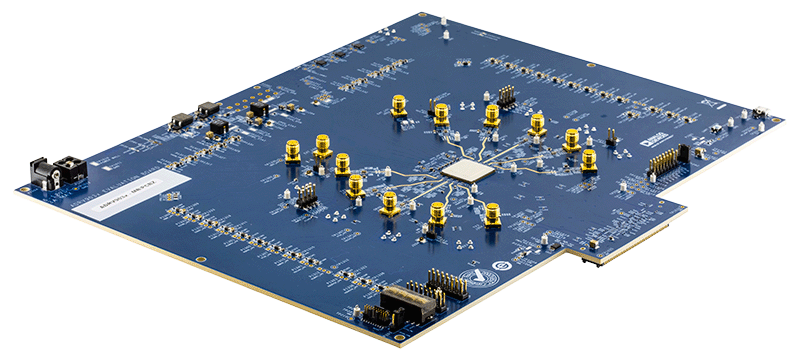
ADS10-V1EBZ Evaluation Board
資料
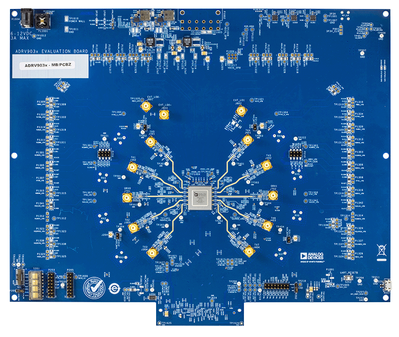
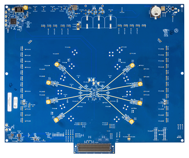
ADRV903x評価システム・ユーザ・ガイド
資料
ソフトウェア
最新のディスカッション
ADRV9032Rに関するディスカッションはまだありません。意見を投稿しますか?
EngineerZone®でディスカッションを始める