
ADPA9005

ADPA9005
新規設計に推奨1GHz to 28GHz, 37.5dBm, GaN Power Amplifier
ADPA9005, 1-28GHz, 37.5dBm PA
- 製品モデル
- 2
- 1Ku当たりの価格
- 最低価格:$712.14
Viewing:
製品情報
- Frequency range: 1GHz to 28GHz
- Internally matched and AC-coupled input and output
- Integrated temperature-compensated RF power detector
- Power gain: 9.5dB typical with PIN = 28.0dBm from 6GHz to 25GHz
- POUT: 37.5dBm typical with PIN = 28.0dBm from 6GHz to 25GHz
- Small signal gain: 20.5dB typical from 6GHz to 25GHz
- OIP3: 39.5dBm typical from 6GHz to 25GHz
- VDD: 20V typical
- IDQ: 560mA
- 14-terminal, 7mm × 7mm, LCC_HS package
The ADPA9005 is a 1GHz to 28GHz, wideband power amplifier with a saturated output power (POUT) of 37.5dBm typical, a power-added efficiency (PAE) of 15.5% typical, and a power gain of 9.5dB typical from 6GHz to 25GHz at an input power (PIN) of 28.0dBm. The RF input and RF output are internally matched and AC-coupled. A drain bias voltage (VDD) of 20V typical is applied to the VDD1 and VDD2 pins, which have integrated bias inductors. The drain current is set by applying a negative voltage to the VGG1 pin. A temperature-compensated RF detector is integrated, which allows monitoring of the RFOUT power.
The ADPA9005 is fabricated on a gallium nitride (GaN) process, is housed in a 14-terminal, ceramic, leadless chip carrier with a heatsink, and is specified for operation from −40°C to +85°C.
APPLICATIONS
- Electronic warfare
- Test and measurement equipment
ドキュメント
データシート 1
ユーザ・ガイド 1
評価用設計ファイル 1
| 製品モデル | ピン/パッケージ図 | 資料 | CADシンボル、フットプリント、および3Dモデル |
|---|---|---|---|
| ADPA9005AEHZ | 14-Terminal LCC_HS (7 mm x 7 mm x 1.063 mm) | ||
| ADPA9005AEHZ-R7 | 14-Terminal LCC_HS (7 mm x 7 mm x 1.063 mm) |
これは最新改訂バージョンのデータシートです。
ソフトウェア・リソース
必要なソフトウェア/ドライバが見つかりませんか?
ドライバ/ソフトウェアをリクエストツールおよびシミュレーション
Sパラメータ 1
評価用キット
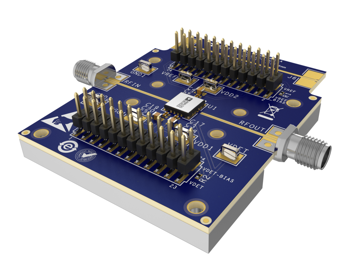
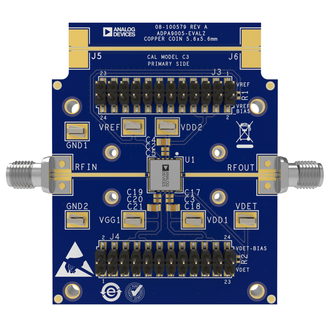
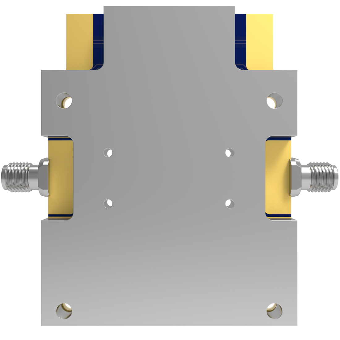
Evaluating the ADPA9005 1GHz to 28GHz, 37.5dBm, GaN Power Amplifier
資料
最新のディスカッション
ADPA9005に関するディスカッションはまだありません。意見を投稿しますか?
EngineerZone®でディスカッションを始める