Overview
Design Resources
Design & Integration File
• Schematic• Bill of Materials
• Gerber Files
• Layout Files (PADs)
• Assembly Drawing Download Design Files 2.32 M
Evaluation Hardware
Part Numbers with "Z" indicate RoHS Compliance. Boards checked are needed to evaluate this circuit.
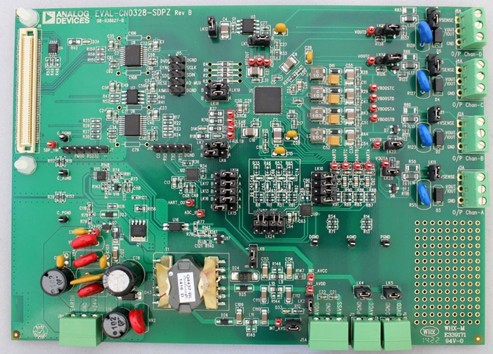
- EVAL-CN0328-SDPZ ($399.30) Completely Isolated 4-Channel Multiplexed HART Analog Output Circuit
- EVAL-SDP-CB1Z ($134.00) Eval Control Board
Device Drivers
Software such as C code and/or FPGA code, used to communicate with component's digital interface.
AD5755 IIO Multi-Channel DAC GitHub Linux Driver Source Code
Features & Benefits
- Complete HART compliant solution for 4mA to 20mA or voltage output
- Fully Isolated
- Four multiplexed outputs
Markets and Technologies
Parts Used
Documentation & Resources
-
CN0328: Completely Isolated 4-Channel Multiplexed HART Analog Output Circuit8/4/2014PDF828 kB
Circuit Function & Benefits
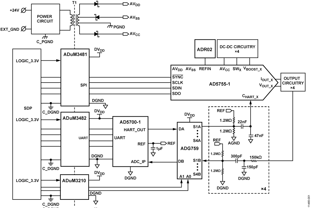
The circuit shown in Figure 1 combines the AD5755-1 (quad channel voltage and current output DAC with dynamic power control) and the AD5700-1 HART modem, to give a completely isolated multiplexed HART®1 analog output solution. Power can be provided either from the transformer isolated power circuit provided on the board (±13 V and +5.2 V outputs, dependent on the load current) or from external power supplies connected to terminal blocks. This circuit is suitable for use in programmable logic controllers (PLCs) and distributed control system (DCS) modules that require multiple HART-compatible 4 mA to 20 mA current outputs, along with unipolar or bipolar voltage outputs. External transient protection circuitry is also included, which is important for applications located in harsh industrial environments.
The AD5755-1 DAC is software configurable and allows the user to easily program the required output ranges and dc-to-dc converter settings used for dynamic power control. It allows access to all of the internal control registers, including the slew rate control register, which is important for applications using HART communication.
The AD5700-1 is the lowest power and smallest footprint HART-compliant IC modem in the industry. It operates as a HART frequency shift keying (FSK) half-duplex modem and integrates all of the necessary signal detection, modulating, demodulating, and signal generation functions. It contains a 0.5% precision internal oscillator, thus reducing board space requirements and cost. The AD5700-1 uses a standard UART interface.
Digital isolation is provided using the quad and dual channel ADuM3481/ADuM3210 digital isolator components based on Analog Devices, Inc., iCoupler® technology. The use of iCoupler technology reduces the need for the additional external components often required in solutions based on optoisolators. An external transformer is used to transfer power across the isolation barrier.
The ADG759 provides multiplexing capability, enabling HART communication, across the four analog output channels. The ADG759 switches one of four differential inputs to a common differential output as determined by the 2-bit binary address lines A0 and A1. When disabled, all channels are switched off. Bypass links are included to provide the flexibility to bypass the multiplexer.
1 HART is a registered trademark of the HART Communication Foundation.
(Simplified Schematic: All Connections and Decoupling Not Shown)
Circuit Description
For industrial control modules, standard analog output voltage and current ranges include ±5 V, ±10 V, 0 V to +5 V, 0 V to +10 V, +4 mA to +20 mA, and 0 mA to +20 mA. The AD5755-1 provides all of these ranges in a high precision, fully integrated, low cost, single-chip solution. A 20% overrange feature is also available for the voltage output ranges. Each DAC channel has a gain (M) and offset (C) register, which allow trimming the gain and offset errors of the entire signal chain.
The current and voltage outputs are available on separate pins, and only one is active at any given time, thus allowing for both output pins to be tied together and connected to a single terminal. When the current output is enabled, the voltage output is in tristate mode, and when the voltage output is enabled, the current output is in tristate mode. Analog outputs are short-circuit and open-circuit protected.
The AD5755-1 allows for an internal or external precision, current setting resistor for the voltage-to-current conversion circuitry, as shown in Figure 3. The stability of the output current value over temperature is dependent on the stability of the value of RSET. As a method of improving the stability of the output current over temperature, an external 15 kΩ low drift resistor can be connected to the RSET_X pin of the AD5755-1 instead of the internal resistor. The external resistor is selected via the DAC control register. Accuracy measurements were evaluated using both options, as described in the Circuit Evaluation and Test section.

Precision Voltage Reference Selection
The AD5755-1 has an on-chip 10 ppm/°C (maximum) reference. For higher performance over temperature, this design uses an ADR02 reference with a 3 ppm/°C maximum drift (B grade, SOIC package). The voltage applied to the reference input is used to provide a buffered reference for the DAC core. Therefore, any error in the voltage reference is reflected in the outputs.
The ADR02 is a 5 V precision reference that allows for an input voltage of up to 36 V. It has a 0.06% maximum accuracy error and a 3 ppm/°C maximum temperature drift (B grade, SOIC package). This drift contributes approximately 0.02% error across the industrial temperature range. It has a long-term drift of 50 ppm (typical) and a 0.1 Hz to 10 Hz noise specification of 10 μV p-p (typical).
Dynamic Power Control
The AD5755-1 contains integrated dynamic power control using a dc-to-dc boost converter circuit, allowing reduced power consumption in the current output mode. Most PLC current output circuits used a fixed voltage source to meet the output voltage compliance requirements across the full range of load resistor values. For example, a 4 mA to 20 mA loop with 750 Ω load, when driving 20 mA, requires a compliance voltage of at least 15 V. However, when driving 20 mA into a 50 Ω load, only 1 V compliance is required. If the 15 V compliance is kept when driving the 50 Ω load, a power dissipation of 20 mA × 14 V = 280 mW is wasted.
The AD5755-1 circuitry eliminates this power loss by sensing the output voltage and regulating the compliance voltage to allow only a small headroom voltage regardless of the load resistance. The AD5755-1 is capable of driving up to 24 mA into a 1 kΩ load.
DC-to-DC Converter Operation
The AD5755-1 contains four independent dc-to-dc converters. These are used to provide dynamic control of the VBOOST_X supply voltage for each channel (see Figure 3). Figure 4 shows the discrete components needed for the dc-to-dc circuitry.

Figure 4. DC-to-DC Circuit
It is recommended to place a 10 Ω, 100 nF low-pass RC filter after CDCDC. This consumes a small amount of power but reduces the amount of ripple on the VBOOST_X supply.
The dc-to-dc converters use a constant frequency, peak current mode control scheme to step up an AVCC input of 4.5 V to 5.5 V to drive the AD5755-1 output channel. These are designed to operate in discontinuous conduction mode (DCM) with a duty cycle of <90% typical.
When a channel current output is enabled, the converter regulates the VBOOST_X supply to 7.4 V (±5%) or (IOUT_X × RLOAD + headroom), whichever is greater. In the current output mode with the output disabled, the converter regulates the VBOOST_X supply to 7.4 V (±5%). In the voltage output mode with the output disabled, the converter regulates the VBOOST_X supply to +15 V (±5%). Full details of the dc-to-dc converter operation can be found in the AD5755-1 data sheet.
HART Coupling
The AD5755-1 has four CHART pins, corresponding to each of the four output channels. A HART signal can be coupled into these pins and appears on the corresponding current output if that output is enabled. Table 1 shows the recommended input voltages for the HART signal at the CHART pin. If these voltages are used, the current output meets the HART amplitude specifications. Figure 5 shows the recommended circuit for attenuating and coupling the HART signals to the AD5755-1 HART inputs.
| RSET | CHART Input Voltage | Current Output (HART) |
| Internal R SET | 150 mV p-p | 1 mA p-p |
| External R SET | 170 mV p-p | 1 mA p-p |

Figure 5. Coupling HART Signal
A minimum capacitance of C1 + C2 is required to ensure that the 1.2 kHz and 2.2 kHz HART frequencies are not significantly attenuated at the output. The recommended values are C1 = 22 nF, C2 = 47 nF. Digitally controlling the slew rate of the output is necessary to meet the analog rate of change requirements for HART.
Digital Slew Rate Control
The slew rate control feature of the AD5755-1 allows the user to control the rate at which the output value changes. This feature is available on both the current and voltage outputs. With the slew rate control feature disabled, the output value changes at a rate limited by the output drive circuitry and the attached load. With the slew rate feature enabled via the SREN bit of the slew rate control register, the output slews between two levels at a rate defined by the SR_CLOCK and SR_STEP parameters accessible via the slew rate control register.
The following equation describes the slew rate as a function of the step size, the update clock frequency, and the LSB size:

where: Slew Time is expressed in seconds.
Output Change is expressed in amps for IOUT_X or volts for VOUT_X.
See the AD5755-1 data sheet for further details.
Transient Voltage Protection
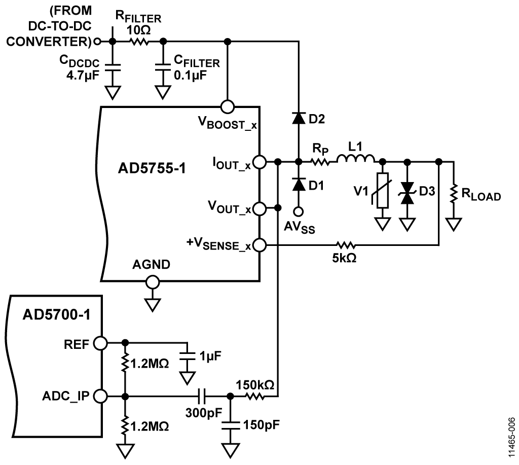
The AD5755-1 contains ESD protection diodes that prevent damage from normal handling. However, the industrial control environment can subject I/O circuits to much higher transients. To protect the AD5755-1 from excessively high voltage transients, a 24 V transient voltage suppressor (TVS) is placed on the IOUT/VOUT connection, as shown in Figure 6. For added protection, clamping diodes are connected from the IOUT_X/VOUT_X pin to the VBOOST_x and AVSS power supply pins. A 5 kΩ current limiting resistor is also placed in series with the +VSENSE_X input. This is to limit the current to an acceptable level during a transient event. The recommended external band-pass filter for the AD5700 HART modem includes a 150 kΩ resistor that limits the current to a sufficiently low level to adhere to intrinsic safety requirements. In this case, the input has higher transient voltage protection and, therefore, does not require additional protection circuitry, even in the most demanding industrial environments.
Input Power Protection
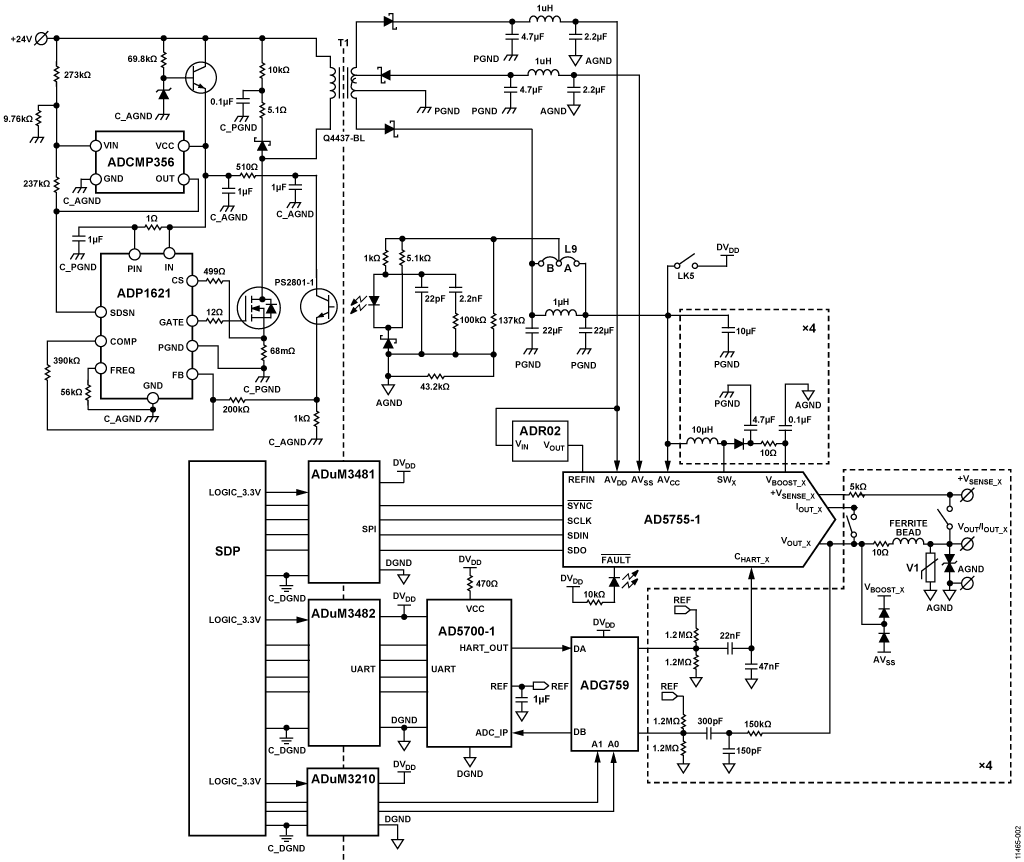
A regulated 24 V dc supply is connected to the board through a 2-wire or 3-wire interface. This supply must be protected against faults and electromagnetic interference (EMI) as shown in Figure 7.

Figure 7. Input Power Transient Voltage Protection
VR1, VR2, VR3, and VR4 are piezoresistors, and F1 is a positive temperature coefficient resistor. This circuit ensures that the evaluation system survives any interference that may be generated on the power ports. See PLC Evaluation Board Simplifies Design of Industrial Process Control Systems, Analog Dialogue 43-04, April 2009, for more details.
The input 24 V supply drives the ADP1621 PWM step-up controller. The controller drives the 3-tap transformer, which provides isolation and generates AVDD (+15 V), AVSS (−15 V), and AVCC (+5 V). The feedback is provided via the PS2801-1 optocoupler.
The ADP1621 supply input voltage range is 2.9 V to 5.5 V, but higher input voltages are possible with the use of a small-signal NPN pass transistor or a single resistor. The switching frequency is set by an external resistor over a range of 100 kHz to 1.5 MHz.
The AVDD, AVSS and AVCC rail voltages are shown in Table 2 under various load conditions.
| Setup | AVDD (V) | AVSS (V) | AVCC (V) |
| Power-circuit unloaded (LK2 to LK5 removed) | +14.7 | -15.3 |
+5.2 |
| LK2 to LK5 inserted; AD5755-1 outputs disabled | +12.5 | -12.6 | +5.2 |
| LK2 to LK5 inserted; AD5755-1 in I OUT mode; 4 mA on 4 channels (500 O load) | +12.7 | -12.8 | +5.2 |
| LK2 to LK5 inserted; AD5755-1 in I OUT mode; 24 mA on 4 channels (1 kO load) | +14 | -15.2 | +5.2 |
| LK2 to LK5 inserted; AD5755-1 in V OUT mode; 10 V on 4 channels (1.2 kO load) | +13 | -13 | +5.2 |
An alternative to using the isolated switching power supply circuit is provided by the J5 and J11 terminal blocks. If these terminal blocks are used, remove LK2 to LK4.
Digital Isolation
The ADuM3481 and ADuM3482 are 3.75 kV quad channel digital isolators in small 20-lead SSOP packages (7.2 mm × 7.8 mm). The isolator core operates between 3.0 V and 5.5 V, whereas the I/O supply can range from 1.8 V to 5.5 V. These devices can be used to interface directly with 1.8 V logic. The ADuM3481 in this design is used to isolate the SPI signals for the AD5755-1 while the ADuM3482 is used to isolate the UART signals for the AD5700-1 HART modem. The dual channel ADuM3210 is used to isolate the address lines of the ADG759 quad channel mux.
Further information on i Coupler products is available at www.analog.com/i Coupler. Complete schematics, bill of materials, and layout files for the EVAL-CN0328-SDPZ board can be found in the CN-0328 design support package.
Common Variations
For applications requiring only current outputs, the AD5757 can be used as an alternative to the AD5755-1. If less than 16 bits of resolution is required, the 12-bit AD5737 can be used.
The AD5700 modem can be used instead of the AD5700-1. However, either an external crystal or a CMOS clock is required, as the AD5700 does not have the internal oscillator option provided on the AD5700-1. See the AD5700 data sheet and the AD5700-1 data sheet for further details.
For single channel applications, see Circuit Note CN0321, Fully Isolated, Single Channel Voltage and 4 mA to 20 mA Output with HART Connectivity.
Circuit Evaluation & Test
A diagram of the basic test setup is shown in Figure 8.
Equipment Required
- The EVAL-CN0328-SDPZ evaluation board
- The CN0328 evaluation software
- The EVAL-SDP-CB1Z system demonstration platform (SDP-B)
- PC (Windows® 32-bit or 64-bit)
- 24 V power supply
- Precision voltmeter, such as Agilent 3458A
- Digital test filter, such as the HCF_TOOL-31 available from the HART Communication Foundation
- 4 each 500 Ω precision load resistors
- Oscilloscope, Tektronix TDS2024B or equivalent
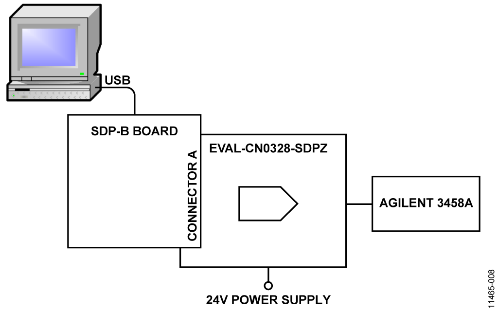
Link Configuration Setup
The default link options are listed in Table 3. By default, the board is configured to be powered by the transformer-isolated supply. The default reference option for the AD5755-1 is the external reference, supplied by the ADR02 (LK1 in position B). LK10 and LK24 are not used by default as these links bypass the ADG759. IOUT_x and VOUT_x are shorted together by default (LK20, LK22, LK23, and LK26).
| Link No. | Default Position | Option | ||||||||||||||||||||
| LK1 | B | This link selects the reference source for the AD5755-1. Position A selects the internal reference on the AD5755-1. Position B selects the ADR02 external reference. |
||||||||||||||||||||
| LK2 | Inserted | This link selects the supply option for AVDD. When this link is inserted, it selects the on-board AVDD, supplied by +24 V supply. It is important that nothing is connected to J5-3 in this instance. When this link is removed, AVDD needs to be driven by an external supply through J5-3. |
||||||||||||||||||||
| LK3 | Inserted | This link selects the supply option for AVSS. When this link is inserted, it selects the on board AVSS, supplied by +24 V supply. It is important that nothing is connected to J5-1 in this instance. When this link is removed, AVSS needs to be driven by an external supply through J5-1. |
||||||||||||||||||||
| LK4 | Inserted | This link selects the supply option for AVCC. When this link is inserted, it selects the on board AVCC, supplied by +24 V supply. It is important that nothing is connected to J11 in this instance. When this link is removed, AVCC needs to be driven by an external supply through J11-1. |
||||||||||||||||||||
| LK5 | Inserted | This link selects the supply option for DVDD. When this link is inserted, it selects that AVCC is tied to DVDD. It is important that nothing is connected to J1 in this instance. When this link is removed, DVDD needs to be driven by an external supply through J1-1. |
||||||||||||||||||||
| LK6 | B | This link selects the logic level for RESET. Position A ties RESET to DGND; in other words, the device is in reset mode. Position B ties RESET to DVDD. |
||||||||||||||||||||
| LK7 | A | This link selects the logic level for POC. Position A ties POC to DGND; the AD5755-1 is powered up with the voltage and current channels in tristate mode. Position B ties POC to DVDD; AD5755-1 is powered up with a 30 kO pull-down resistor to ground on the voltage output channel, and the current channel is in tristate mode. |
||||||||||||||||||||
| LK11, LK21, LK25, LK8 | Inserted | These links connect the +VSENSE input to VOUT/IOUT for Channel A, Channel B, Channel C, and Channel D, respectively. When this link is inserted, the +VSENSE input is connected directly to the VOUT/IOUT pin. When this link is removed, the +VSENSE input is left floating and must be connected to the high-side of the load resistance external to the evaluation board. | ||||||||||||||||||||
| LK9 | A | This link selects the feedback node to the ADP1621. Note that this link must not be dynamically changed while the board is powered up. Position A selects the AVCC node after the filter circuit. Position B selects the pre-filtered AVCC node. |
||||||||||||||||||||
| LK10, LK24 | Removed | These links select which channel bypasses the ADG759 (use only when ADG759 is not in use). Position A selects channel A. Position B selects channel B. Position C selects channel C. Position D selects channel D. |
||||||||||||||||||||
| LK12 | Inserted | When inserted, the AVDD supply is connected to the ADR02 supply, thus powering the on-board 5 V reference. | ||||||||||||||||||||
| LK13, LK14 | A | These links select the address of the ADG759.
|
||||||||||||||||||||
| LK15 | B | ADG759 enable. Position A = mux disabled. Position B = mux enabled. |
||||||||||||||||||||
| LK16, LK17 | A | These links select the source of control for the ADG759 address pins. Position A selects SDP control. Position B selects LK13/LK14 control. |
||||||||||||||||||||
| LK18, LK19 | A | These links control the address pins for the AD5755-1.
|
||||||||||||||||||||
| LK20, LK22, LK23, LK26 | Inserted | When these links are inserted, VOUT and IOUT of the AD5755-1 are shorted together, for Channel A, Channel B, Channel C, and Channel D, respectively. |
Power Supply Configuration
By default, the board is configured to be powered by the transformer-isolated supply, therefore, links LK2 to LK5 are inserted. If the terminal blocks are used to provide power to the circuit, the following supplies must be provided:
- ±15 V to AVDD/AVSS on Connector J5. This supplies both the AD5755-1 and the ADR02 reference.
- 4.5 V to 5.5 V to AVCC on Connector J11 for the AVCC supply of the AD5755-1.
- With LK5 in place, the EXT_AVCC supply also supplies DVDD. DVDD is used to power the digital supply of the AD5755-1 and provides power for the AD5700-1 HART modem, the ADG759 mux, and the secondary side of the isolator devices. Alternatively, DVDD (2.7 V to 5.5 V) can be supplied by an external supply connected to J1.
Software Installation
The evaluation kit includes self-installing software on a CD. The software is compatible with Windows XP (SP2), Vista (32-bit and 64-bit) or Windows 7 (32-bit and 64-bit). If the setup file does not run automatically, run the setup.exe file from the CD.
Install the evaluation software before connecting the evaluation board and SDP board to the USB port of the PC to ensure that the evaluation system is correctly recognized when connected to the PC.
- Connect the EVAL-SDP-CB1Z via the USB port of the PC using the supplied cable.
- Connect the EVAL-CN0328-SDPZ evaluation board to Connector A. If Connector B is used, the UART of the EVAL-SDP-CB1Z does not function as required.
- Power up the EVAL-CN0328-SDPZ by applying 24 V to the J9 connector.
- Start the EVAL-CN0328-SDPZ software and proceed through any dialog boxes that appear. This completes the installation.
Software
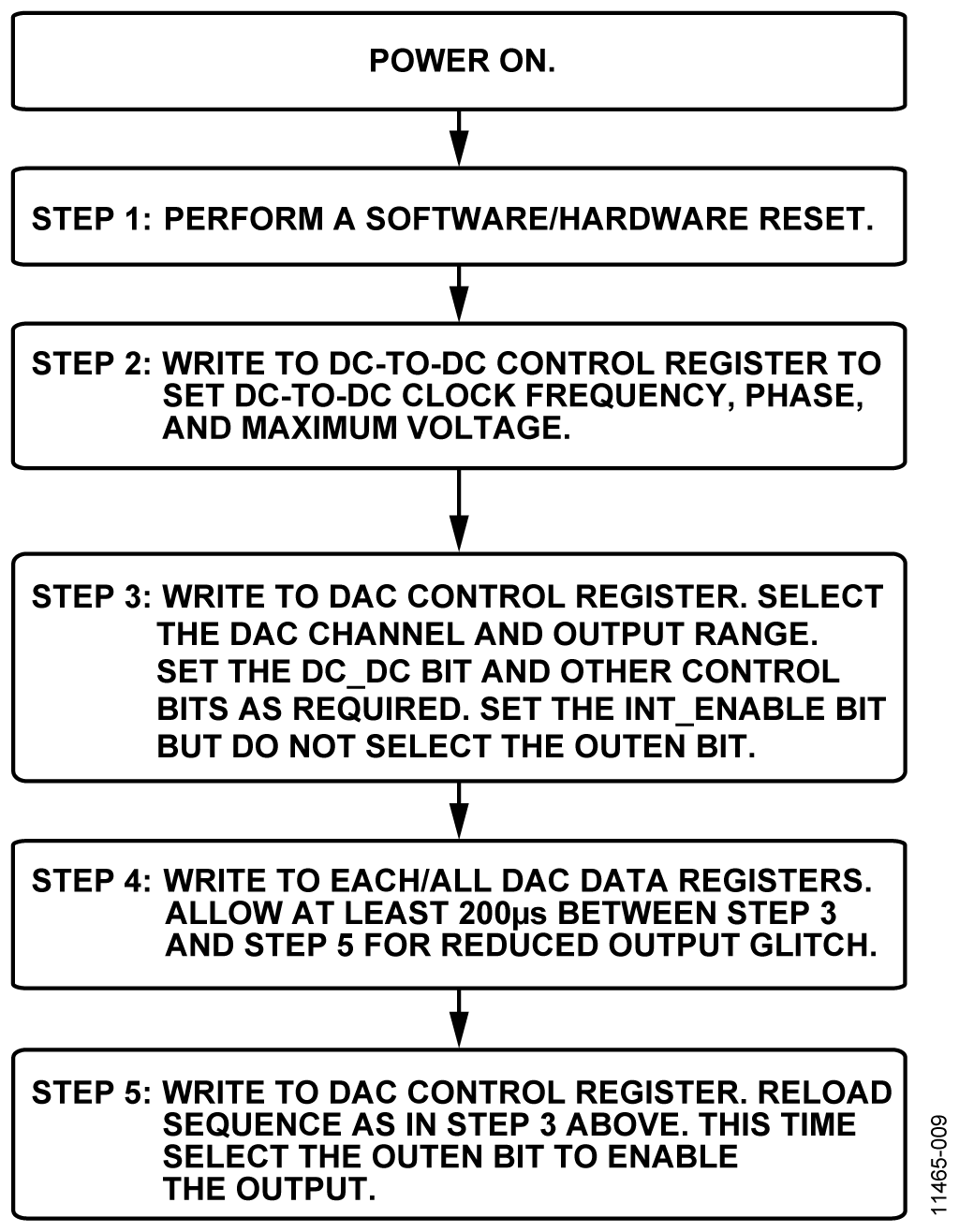
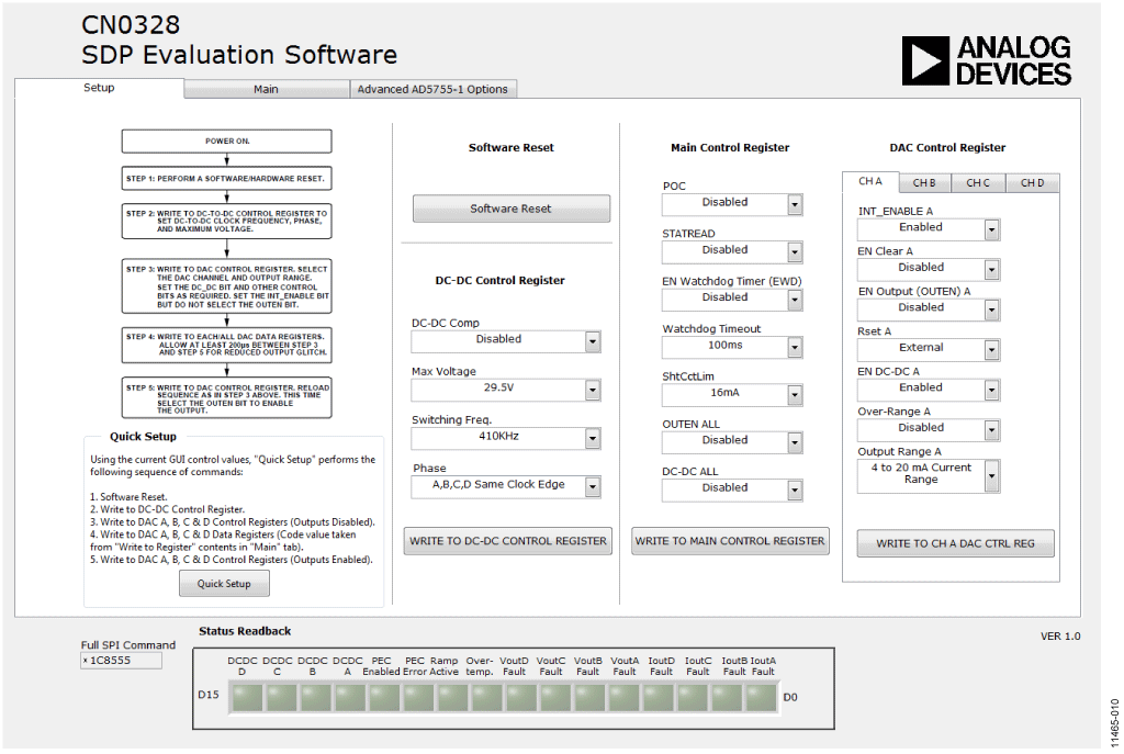
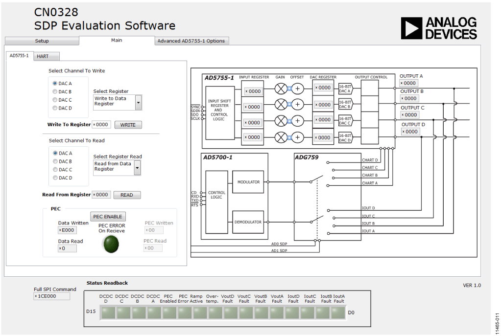
The main software window is shown in Figure 10. Use the setup tab initially to set up the AD5755-1 in the recommended fashion by first setting up the dc-to-dc control settings, followed by the DAC control settings, then loading the required code to the data registers and finally enabling the outputs (see Figure 9). A quick setup feature is provided in the setup tab to aid correct programming of the AD5755-1. For HART communications, ensure a current output range is enabled. The main tab can then be used to issue a HART command and/or update the AD5755-1 output code.
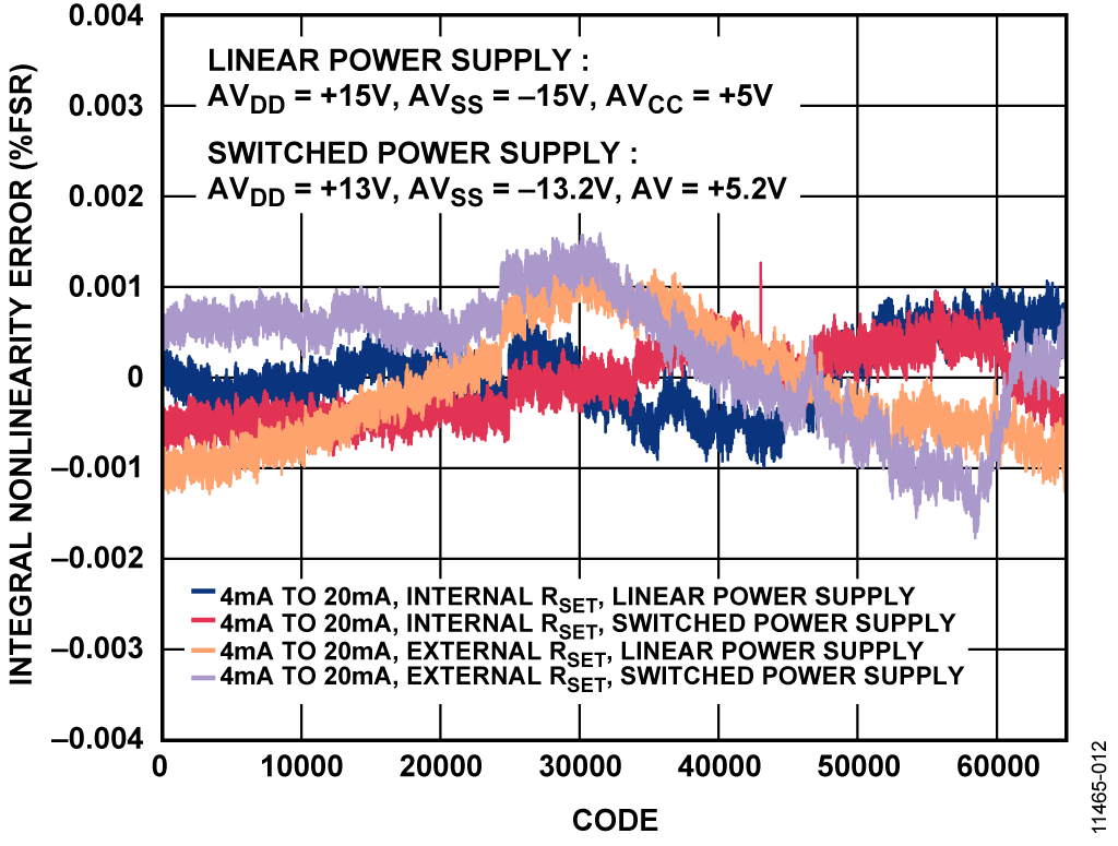
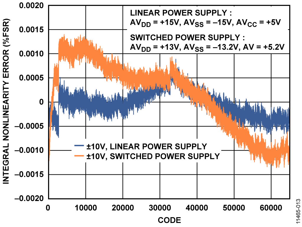
The INL of the AD5755-1 was tested using both linear power supplies and the transformer isolated switched power supplies. As shown in Figure 12 and Figure 13, there is no noticeable performance loss in system accuracy using the switched power supplies versus the linear power supplies. The AD5755-1 data sheet specifies an INL of ±0.006% FSR across the full temperature range for both IOUT and VOUT irrespective of whether RSET internal or external is used. The plots show that the measured results fall well within this specification.
Absolute Accuracy Performance
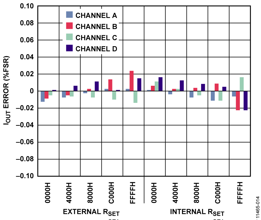
The specification for the total unadjusted error (TUE) for the AD5755-1 in current output mode using the internal RSET is ±0.11% FSR maximum at 25°C. The total error of the ADR02 reference (B grade) is 0.06% maximum at 25°C.
Table 4 shows the measured current output error of the circuit for Channel A in the 4 ma to 20 mA range with a 500 Ω load using internal RSET. Figure 14 summarizes the results for all four channels, using both internal and external RSET. All results are within the expected values.
| Code (Hex) | IOUT (mA) | Error (% FSR) |
| 0000 | 4.0002 | +0.0013 |
| 4000 | 7.9994 | -0.0038 |
| 8000 | 11.9988 | -0.0075 |
| C000 | 15.9982 | -0.0112 |
| FFFF | 19.9990 | -0.0063 |
Similar measurements were taken for the voltage output mode, where the AD5755-1 TUE specification is ±0.03% FSR maximum at 25°C. Table 5 shows the results for Channel A. The remaining three channels showed similar results.
| Code (Hex) | VOUT (V) | Error (% FSR) |
| 0000 | -10.0032 | -0.0160 |
| 4000 | -5.0017 | -0.0085 |
| 8000 | 0.000326 | 0.0016 |
| C000 | 5.0007 | 0.0035 |
| FFFF | 10.0015 | 0.0075 |
HART Compliance
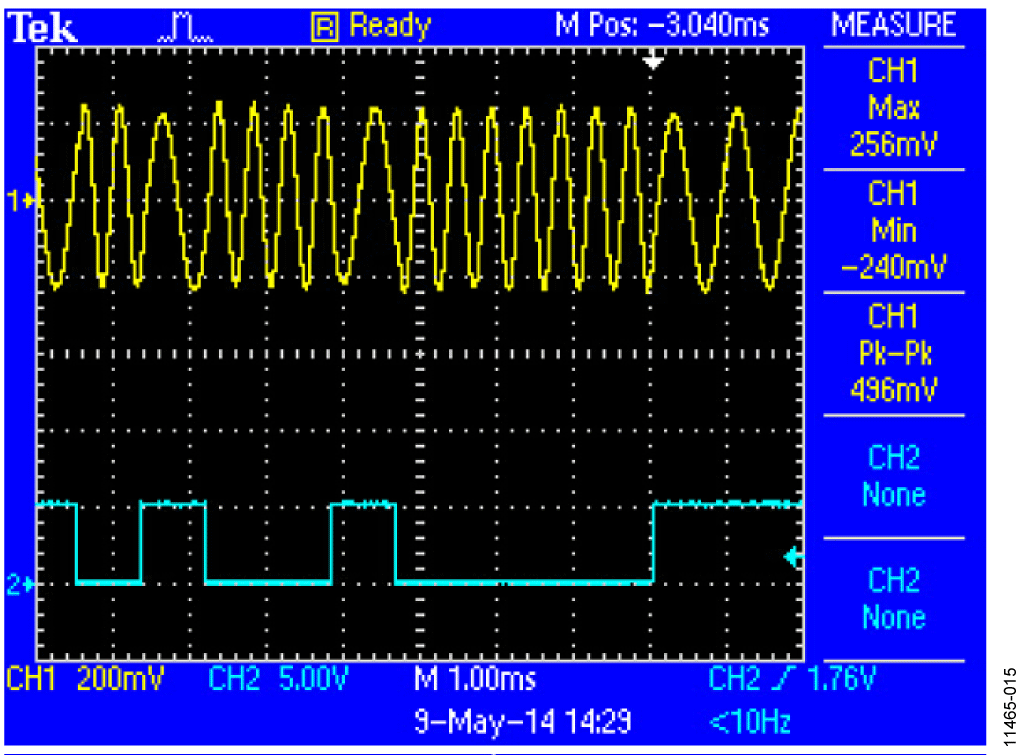
Figure 15 shows the 1200 Hz and 2200 Hz FSK frequencies measured across a 500 Ω load resistor on IOUT_A. Channel 1 shows the modulated HART signal coupled into the AD5755-1 output (set to 4 mA), while Channel 2 shows the AD5700-1 TXD signal.
For the circuit in Figure 2 to be HART-compliant, it must meet the HART physical layer specifications. There are numerous physical layer specifications included in the HART specification documents. For evaluating the performance of the hardware, the two specifications considered here are the output noise during silence and the analog rate of change.
Output Noise During Silence Test
When a HART device is not transmitting (silent), it does not couple noise onto the network in the HART extended frequency band. Excessive noise may interfere with reception of HART signals by the device itself or other devices on the network.
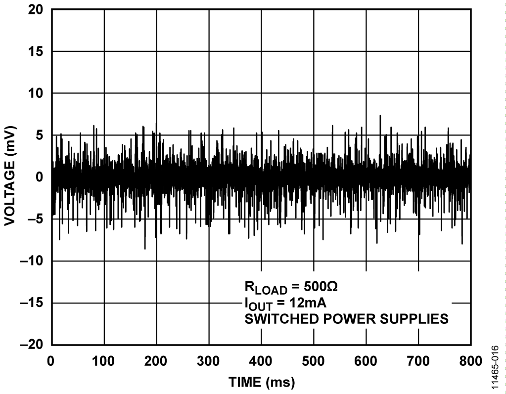
The voltage noise measured across a 500 Ω load must contain no more than 2.2 mV rms of combined broadband and correlated noise in the HART extended frequency band. Additionally, the noise must not exceed 138 mV rms outside of this frequency band.
This noise was measured by connecting the HCF_TOOL-31 filter (available from the HART Communication Foundation) across the 500 Ω load and subsequently connecting the output of the filter to a true rms meter. An oscilloscope was used to examine the output waveform.
Like the earlier linearity tests, this test was performed using both the linear and isolated switched power supplies. While noise results obtained using the linear power supplies were much lower than those obtained using the isolated switched power supplies, both were within the required HART specification.
| Output Noise | Inside Extended HART Frequency Range (<2.2 mV Limit) (mV rms) | Outside Extended HART Frequency Range (<138 mV Limit) (mV rms) |
| Linear Power Supplies | 0.06 | 0.5 |
| Switched Power Supplies | 0.3 | 2.7 |
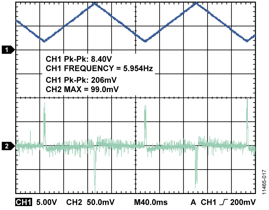
Analog Rate of Change
This specification ensures that when a device regulates current, the maximum rate of change of analog current does not interfere with HART communications. Step changes in current disrupt HART signaling. The worst-case change in the analog output current must not produce a disturbance higher than 15 mV peak, measured across a 500 Ω load in the HART extended frequency band. Meeting this requirement ensures that the maximum bandwidth of the analog signaling is within the specified dc to 25 Hz frequency band. For this test, the HCF_TOOL-31 was again connected across the 500 Ω load, as in the noise during silence test, and an oscilloscope was connected to its output. Rather than setting the AD5755-1 output to a fixed output current, this time the AD5755-1 was programmed to output a cyclic waveform, switching from 4 mA to 20 mA. To meet the required system specifications, the output current change was limited by the digital slew rate control feature of the AD5755-1. This feature is described in more detail in the Digital Slew Rate Control section and in the AD5755-1 data sheet. For this test, SR_CLOCK and SR_STEP were set to 64 kHz and 16 LSBs respectively, giving a slew time of 64 ms. The result is shown in Figure 17. Channel 1 shows the AD5755-1 IOUT_A signal stepping between 4 mA and 20 mA, sensed across the 500 Ω load and connected to the input to the bandpass filter. The output of the filter (which has a gain factor of 10) can be seen on Channel 2. The peak value is within the previously mentioned 150 mV peak limits.
