Overview
Design Resources
Design & Integration File
- Schematic
- Bill of Materials
- Gerber Files
- Allegro Files
- Assembly Drawing
Evaluation Hardware
Part Numbers with "Z" indicate RoHS Compliance. Boards checked are needed to evaluate this circuit.
- EVAL-ADICUP360 ($60.92) Arduino Form Factor Compatible Development System
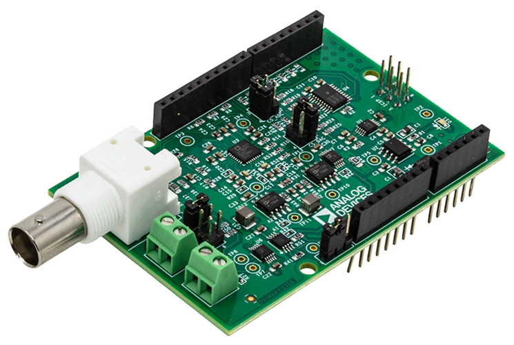
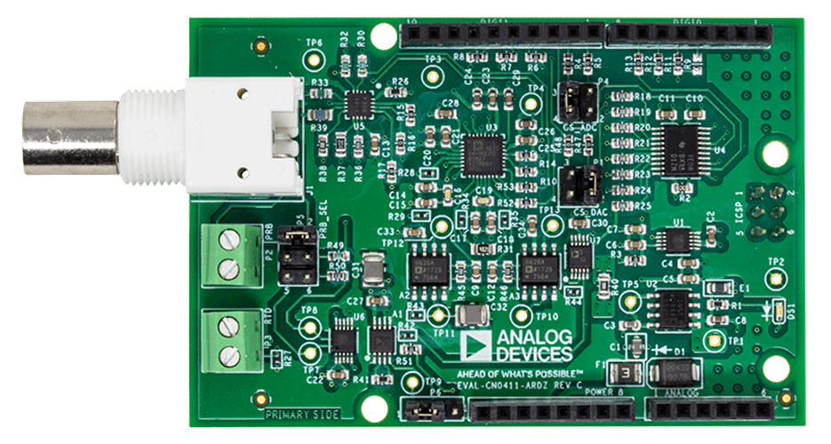
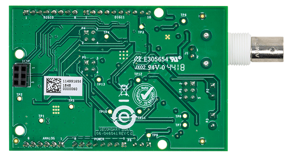
- EVAL-CN0411-ARDZ ($94.75) Total Dissolved Solids Measurement Board
Device Drivers
Software such as C code and/or FPGA code, used to communicate with component's digital interface.
AD5686 GitHub Linux Driver Source Code (SPI)
nanoDAC+ GitHub no-OS Driver Source Code
Features & Benefits
- Measures TDS using Electrical Conductivity
- Measurement range from 1uS to 1S
- Uses Standard BNC Probe Connection
- Arduino Form Factor Compatible
Markets and Technologies
Parts Used
Documentation & Resources
-
cn0411 User Guide12/12/2018WIKI
-
CN0411: TDS Measurement System for Water Quality Monitoring (Rev. 0)12/13/2018PDF257K
Circuit Function & Benefits
The total dissolved solids (TDS) present in a water system is composed of inorganic salts and small amounts of organic matter that are dissolved in water, and is an important measure of water quality. TDS can be derived from the electrical conductivity (or conductivity) of the solution by a factor dependent on the properties, temperature and, number of ions present. By measuring the conductivity of the solution, determining the TDS of the system is faster, economical, and less complicated in contrast to the more accurate gravimetric method. The latter method involves evaporating the water and weighing the residue, which is applicable in laboratory settings but impractical in the field.
The circuit shown in Figure 1 is a TDS measurement system based on the conductivity of the solution. This design uses a combination of components that allow for single-supply operation, which minimize circuit complexity, making this suitable for low-power and portable instrument applications.
The simplest method of measuring the conductivity of the solution uses a 2-wire conductivity cell. Conductivity measurements require temperature compensation for measurements taken at temperatures other than 25˚C (or other reference temperature). This system can reference the conductivity measurement to room temperature using either a 100 Ω or 1000 Ω, 2-wire resistance temperature device (RTD) and can accommodate 2-wire conductivity cells of various cell constants and operating parameters.
The capacitance and polarization effects of the electrodes in the conductivity cell require that the excitation signal be a bipolar square wave with a sufficiently high frequency to reduce polarization effects but also with sufficiently long periods to reduce capacitance effects. To avoid damaging the conductivity electrodes, the signal must have a very low to zero dc offset and magnitude.
The circuit can measure the range of conductivity values from 1 µS to 0.1 S. A multiplexer switches between seven precision resistors of different values to set the gain when measuring the conductivity probe signal. The system can automatically determine the gain setting of the conductivity measurement through an auto-ranging procedure implemented in software. The system can also be calibrated in the high conductivity range to increase its accuracy.

Circuit Description
Conductivity and Total Dissolved Solids Theory
The TDS in a solution is largely composed of inorganic salts that separate into ions in the presence of a polar solvent like water. When a potential is applied to the solution via two electrodes, the movement of the ions constitutes a current that, when there is negligible electrolysis, obeys Ohm’s law. The resistance, R, of the solution can then be calculated by Equation 1.

where:
V is the potential difference applied to the two electrodes.
I is the measured current across the two electrodes.
ρ is the resistivity of the material in Ω cm.
L is the distance between the two electrodes.
A is the area of the electrodes.
The conductance, G, is the reciprocal of resistance and measured in Siemens (S), and conductivity, Y, is the reciprocal of resistivity and measured in S/cm, mS/cm, or µS/cm. Rearranging Equation 1, the conductance can be obtained from the potential across the two electrodes and the current through them. Conductivity is the conductance multiplied by a factor related to the geometry of the electrodes (see Equation 2).

Typically, conductivity is measured using a 2-electrode sensor called a conductivity probe or conductivity cell. An excitation voltage is applied to the conductivity cell while it is immersed in the solution as shown in Figure 2.

The conductivity cell constant or simply cell constant, KCELL, is the ratio of the gap between its two electrodes and the area of each electrode, which shortens Equation 2 to Equation 3. The cell constant has a unit of cm−1 but the unit may be omitted by manufacturers of conductivity probes.

The typical measurement system computes conductance from the current and voltage readings. Since the conductivity range of values is very large, measuring conductance at the extremes (values less than 1 µS and greater than 0.1 S) can be difficult for ordinary instruments. By choosing a conductivity cell with an appropriate cell constant, the range of conductivity measurement can be extended. Conductivities less than 0.1 µS/cm can be measured at a lower conductance by using a conductivity cell with a lower cell constant. Conversely, conductivities greater than 0.1 S/cm can be measured at a higher conductance by using a conductivity cell with a higher cell constant. Typical values of the cell constant used for a corresponding range of conductivity measurement is shown in Table 1.
| Cell Constant | Range of Measured Conductivity |
| 0.01 | < 0.1 µS/cm |
| 0.1 | 0.1 µS/cm to 100 µS/cm |
| 1 | 100 µS/cm to 10 mS/cm |
| 10 | 10 mS/cm to 1 S/cm |
Each conductivity cell has a rated excitation voltage, which must not be exceeded so as not to damage the electrodes. Do not apply a dc voltage to any of the electrodes.
Dielectric Properties
Polarization and the dielectric properties of the solution primarily affect the accuracy of the measured voltage signal across and the current through the conductivity cell. Polarization arises from the accumulation of ions and the chemical reactions that occur near the electrode surface. The dielectric properties of the solution contribute to a frequency dependent impedance and interelectrode capacitance. A technique used to maximize the accuracy of the conductance measurement uses a bipolar pulse excitation. An excitation voltage +VEXC is applied for time t1 then the opposite excitation voltage −VEXC is applied for time t2. Also, t1 and t2, and +VEXC and −VEXC must be equal with no greater than 1% difference in duration and magnitude, respectively. The frequency of the signal (t1 + t2) −1 must be adjusted to the range of conductance measurement. Typically, this is 94 Hz in the µS range and 2.4 kHz in the mS range. These frequencies are compromises that minimize the effect of interelectrode capacitance, while preventing the accumulation of ions on the electrode surface.
Conductivity Measurement
The front-end of the conductivity measurement can be simplified to a voltage divider network as shown in Figure 3.

RGAIN sets the magnitude of the voltage across and current through the conductivity cell and solution simplified as RCOND.
Node B and Node C are constantly switched to impose a bipolar square wave across RCOND. A multiplexer switches between different gain resistors in Node A.
The applied excitation voltage at Node A to the voltage divider is generated using AD5683R, a 16-bit SPI voltage digital-to-analog converter (DAC). This allows the magnitude of the square wave signal applied to the voltage divider to be user-configurable. Choose the excitation voltage to maximize the signal while not exceeding the probe’s ratings. By default, the software applies 0.4 V excitation. The AD5683R is also by default the source of the system’s 2.5 V reference voltage, but can also be configured to accept an external reference voltage.

Figure 4 shows the gain setting resistors and switch, where R1 = 20 Ω, R2 = 200 Ω, R3 = 2 kΩ, R4 = 20 kΩ, R5 = 200 kΩ, R6 = 2 MΩ, R7 = 20 MΩ and P1, P2, and P3 are GPIO outputs from the AD7124-8.
The circuit has a usable conductance range of 1 µS to 1 S. The voltage divider of the conductivity cell scales through these ranges by switching between seven gain resistors using ADG1608 as shown in Figure 4. The ADG1608 is an 8-channel multiplexer with a typical on-resistance of 12.5 Ω when operating at a single 5 V supply. This on-resistance is significant when the conductivity measurement is in the 20 to 200 Ω range. Pin S2 and Pin S3 of the ADG1608, which connect to the 20 Ω and 200 Ω gain resistors, respectively, are also connected to two input channels of the analog-to-digital converter (ADC). The system can also be configured to perform an initial calibration for measurement errors in the 20 and 200 Ω range. Shown in Figure 5 is a 3-option (6-pin) jumper selection header (P5), which connects to 20 Ω and 200 Ω precision resistors. Shorting Pin 1 and Pin 2 configures the system to measure the signal across the conductivity cell while shorting Pin 3 and Pin 4 or Pin 5 and Pin 6 configures the system to measure the signal across the precision resistors.

The conductivity cell is switched to impose a bipolar signal across it using an ADG884 as shown in Figure 6. The ADG884 has 0.5 Ω typical on-resistance and is operating at a single 3.3 V supply. The switching is controlled by a PWM signal from the microcontroller board. The frequency of this signal is userconfigurable to 94 Hz for low conductivity measurements and 2.4 kHz for high conductivity measurements.

The signal across the conductivity cell is amplified by a gain of 10 using the AD8220 low input bias current instrumentation amplifier operating at a single 5 V supply with input signals up to 0.25 V as shown in Figure 7. There is also a user-configurable jumper selector P6, which provides for a system zero-scale calibration.

The output of the instrumentation amplifier passes through two parallel sample-and-hold circuits. As shown in Figure 8, the sampling of the AD8220 output is controlled by the ADG836, a dual SPDT switch, which has low charge-injection and is operating at a single 3.3 V supply with input signals of up to 2.5 V.
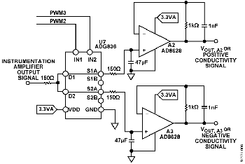
The switch connects the two parallel sample-and-hold circuits using PWM1 and PWM2 at the middle of the positive and negative cycles of the main PWM1 signal. The switching diagram for the three PWM signals and the voltage across the conductivity cell is shown in Figure 9.

This sampling method decreases the electrode capacitance effects at the beginning of the PWM1 signal state change as well as the electrode polarization effects occurring at the end of each state. This causes the output of the sample-and-hold circuit to be two dc levels corresponding to ten times the positive and negative voltage values across the conductivity cell, respectively.
The maximum charge injection due to the switching is 40 pC, which constitutes an error of 40 pC ÷ 47 µF ≈ 851 nV. The worst case drop voltage is the product of half the period of the low frequency switching and the droop rate, which is the worst-case leakage current of the ADG836 and the worst-case bias currents of the AD8628 divided by the hold capacitance. As shown in Equation 4, this drop voltage is theoretically 23 nV.

The outputs of A2 and A3 AD8628 buffer amplifier are applied to the single-ended ADC AD7124-8 input channels, AIN7 and AIN8, respectively. These input channels are referenced by default to the AD5683 reference voltage. AD7124-8 is userconfigurable to perform either single or continuous sampling. It is also user-configurable to perform a system zero-scale calibration using the selectable precision resistors in P5 or read the multiplexer on-resistance using the input channels from the 20 Ω and 200 Ω gain resistors.
The positive and negative output voltages is computed from the 24-bit unipolar ADC code using Equation 5.

where:
ADCCODE is the 24-bit unipolar code of the signal sample.
VREF is by default 2.5 V
Equation 6 shows the calculation of the peak-to-peak voltage across the conductivity cell from the AD8628 output voltages.

The current through the conductivity cell can be calculated from the peak-to-peak cell voltage, gain resistance, and excitation or DAC voltage using Equation 7.

The conductivity YSOL of the solution is given by Equation 8.

where KCELL is the conductivity cell constant.
Substituting Equation 7 and Equation 8 into Equation 9 yields the following equation:

Equation 9 shows that the conductivity measurement depends on the conductivity cell constant, the excitation voltage, the gain resistance used and the sum of the two voltage outputs of each sample-and-hold channel.
Temperature Compensation
Conductivity measurements are also temperature dependent; conductance increases as temperature increases. Most commercial conductivity probes have an integrated RTD, facilitating temperature compensation.
The typical method to compensate the conductivity measurement to a standard reference temperature is through a linear function dependent on the temperature coefficient α, which is based on the type of ions present in the solution as shown in Equation 10. Usually, the reference temperature is set at 25 ˚C.

where:
YREF is the conductivity referenced to TREF.
Y is the conductivity at temperature T.
TREF is the reference temperature.
T is the solution temperature.
α is the temperature coefficient
The typical values of α for common salt solutions are shown in Table 2.
| Salt Solution | Temperature Coefficient (α) |
| Potassium Chloride (KCl) | 1.88 |
| Sodium Chloride (NaCl) | 2.14 |
The TDS of the solution in mg/L is calculated from the referenced conductivity measurement using Equation 11.

where ke is the TDS factor.
The TDS factor is calculated by measuring the referenced conductivity of a standard known TDS solution as shown in Equation 12.

where:
TDSREF,STD is the known TDS value of the solution at TREF. YREF,STD is the measured conductivity of the solution at TREF.
The conductivity measurement cannot distinguish between constituents and individual types of ions. Thus, the TDS factor varies at a specific range, which is distinct for each type of solution. Table 3 shows the typical range of the TDS factors of common salt solutions.
| Salt Solution | Range of TDS Factor (ke) |
| Potassium Chloride (KCl) | 0.50 to 0.57 |
| Sodium Chloride (NaCl) | 0.47 to 0.50 |
Temperature Measurement
Conductivity varies significantly with the temperature of the solution and the temperature coefficients are also significantly for each type of solution. A simple method of measuring the temperature of a solution uses a 2-wire RTD. The simplified front-end schematic is shown in Figure 10.

The AD7124-8 contains two matched software configurable constant current sources, which have eight selectable current output values and can be made available to any of the analog input channels. The excitation current to the RTD resistor network is set to 250 µA from the AIN0 channel. Node A and Node B are connected to the AD7124-8 external reference input. Node B and Node C, which constitute the differential RTD signal, are connected to the AD7124-8 analog input channels. Both differential inputs are passed through two identical and typical RC low-pass filter as shown in Figure 11.

This low-pass filter topology provides attenuation of both differential and common-mode noise signals. The large value of R1 and R2 in Figure 11 also help to protect against 30 V miswiring.C1 and C2 are the common-mode capacitors and are set to a tenth of the differential-mode capacitor C3. This attenuates the effects of noise due to mismatch between the common-mode capacitors. The common mode cut-off frequency (fCM) is approximately 20 times the differential mode cut-off frequency (fDM), which are 53 kHz and 2.5 kHz, respectively. The calculations are shown in Equation 13.

where:
fCM is the common mode cut-off frequency.
fDM is the differential mode cut-off frequency.
All resistance values for the RTD are referenced or capped to 4.02 kΩ and the reference voltage is 250 µA × 4.02 kΩ = 1.005 V.
Also, the system can accommodate both Pt100 or Pt1000 RTDs. The resistance of the RTD (RRTD) is computed from the 24-bit unipolar ADC code using Equation 14.

where:
ADCCODE is the 24-bit unipolar code of the signal sample. RREF is the reference resistor. RREF = 4.02 kΩ.
The Callender-Van Dusen equation is used to define the relation of the RTD resistance and temperature. For temperatures greater than or equal to 0˚C or for resistances greater than or equal to R0, the temperature in degrees Celsius can be computed using Equation 15, which can be obtained directly from the Callender-Van Dusen equation.

where:
A = 3.9083 ×10⁻³ .
B = −5.775 ×10⁻⁷ .
C = −4.183 × 10⁻¹².
R0 is the RTD resistance at 0˚C.
RRTD is the RTD resistance at TRTD.
TRTD is the temperature in degrees Celsius.
For temperatures below 0˚C or for resistances below R0, a best fit polynomial expression is used as shown in Equation 16.

where:
C1 = -242.02
C2 = 2.2228
C3 = 2.589 ×10⁻³
C4 = 48.26 × 10⁻³
C5 = 1.5243 × 10⁻¹⁰
RRTD is the RTD Resistance at TRTD.
TRTD is the temperature in degrees Celsius.
Software Operation Settings
The provided software configures six parameters for TDS measurement:
- Conductivity cell excitation voltage
- Gain resistance selected by the multiplexer
- Value of RTD used
- Conductivity cell switching frequency
- Conductivity probe cell constant
- Type of solution being measured.
The DAC voltage can be set to any value from 0 to 2.5 V. At startup, the DAC voltage is set to 400 mV.
The selected gain resistance can be set to open or any of the seven resistor values: 20 Ω, 200 Ω, 2 kΩ, 20 kΩ, 200 kΩ, 2 MΩ, and 20 MΩ. Initially, the gain resistance is set to open.
The type of RTD used can be set to either Pt100 or Pt1000. Initially, the type of RTD used in temperature measurements is set to Pt100.
The frequency of the PWM signal sets the frequency of the bipolar pulse across the conductivity cell. The software can only switch between two options for PWM frequency: 94 Hz and 2.4 kHz. Initially, the PWM frequency is set to 94 Hz.
There are three fixed options for conductivity probe cell constants: 0.1, 1.0, and 10. A forth option allows the user to enter a custom value for probes with cell constants other than 0.1, 1.0, and 10. By default, the cell constant is set to 1.0.
The type of solution sets the TDS factor and temperature coefficient used in computing for TDS and temperature compensation, respectively. The software has built-in settings for only sodium chloride (NaCl) and potassium chloride (KCl) solutions. However, the user can set custom values for the TDS factor and temperature coefficient separately for other types of solutions. Initially, the type of solution is set to NaCl.
Apart from these parameters, the software can also switch between taking measurements with the ADC in single conversion mode and with the ADC in continuous conversion mode. In single conversion mode, the ADC goes to idle mode whenever a read conductivity command is not being issued. This decreases the power consumption of the board when it is not active. Additionally, the DAC voltage value can be set to zero in these times to further decrease the board’s consumption. In continuous conversion mode, the ADC continuously samples the conductivity cell signal. This decreases the measurement time for each sample, which makes this effective when continuously monitoring the conductivity of a solution.
Auto-Ranging Conductivity Measurement
For a given type of solution and conductivity probe used, the range of conductivity measurement range encompasses multiple gain resistance settings. Furthermore, to prevent the excitation voltage from exceeding the rated voltage of the conductivity cell, the excitation voltage value must change along with the gain resistance. The software is capable of automatically setting the gain resistance and the excitation voltage to the range of the conductivity of the solution. This ensures that the conductivity reading is always being measured at the most reliable setting. The method of auto-ranging the conductivity measurement is described in Figure 12.

Calibration Procedure
The system is capable of two calibration methods, a zero-scale calibration and through a reference precision resistance. The calibration method used to obtain the measurements discussed in Figure 15 uses a reference precision resistance, which can either be a 20 Ω or 200 Ω resistor as shown in Figure 5. It is in these resistance ranges that the on-resistance of the multiplexer has a significant effect on the conductivity measurement. The output of this calibration is an offset resistance value, which is added to the gain resistance used in the computation of conductivity. Figure 13 shows the procedure to perform this calibration.

The zero-scale calibration performs the zero-scale calibration of the AD7124-8, which eliminates the output bias voltages of the sample-and-hold topology. This ensures that a zero-input to the conductivity cell corresponds to the ADCs zero code. Place a shunt in Pin 2 and Pin 3 of Jumper Header P6 of the CN-0411 board. The AD7124-8 is commanded to perform system zeroscale calibration on both the positive and negative voltages of the conductivity signal. This stores the zero-input voltage level in the ADCs offset registers and is automatically considered in every sample reading.
Both these two calibration methods need to be done only once for each board since the software stores the output of the calibration procedures.
System Accuracy
From Equation 9, the computation of conductivity depends on the two output voltages of the sample-and-hold topology, RGAIN, and the DAC output voltage. RGAIN resistors below the MΩ range have 0.1% tolerance while the 2 MΩ and 20 MΩ resistors have 1% tolerance. Added to the resistances in the simple voltage divider network shown in Figure 3 are the onresistances of the multiplexer ADG1608 and the conductivity cell switch ADG884, which are maximum at 17.4 Ω and 0.96 Ω, respectively. The input bias currents and input offset current from the instrumentation amplifier introduces a voltage, which scales with the gain resistance and the resistance of the solution. The B-grade AD8220 has a max input bias current of 10 pA for each input and a max input offset current of 0.6 pA, which makes a total input bias current of 20.6 pA. At 20 MΩ, this constitutes a 20.6 pA × 20 MΩ = 412 µV input bias voltage. Moreover, at a gain of 10, the AD8220 has a 0.2% max gain error. Computing conductivity directly from a known precision resistance measures the system accuracy and accounts for all these factors, including the ones introduced by the sample-andhold topology, such as the drop voltage in Equation 4.
Figure 14 shows the measured accuracy of the conductivity measurements taken using precision resistors from 1 MΩ to 10 Ω, corresponding to conductivities of 1 µS to 0.1 S. An increase in the system errors is visible in the 10 mS to 100 mS range. For these ranges, a calibration method to on-board precision resistances (shown in Figure 5) is required.

Calibration is performed only once for each board and an offset resistance is obtained, which accounts for the on-resistance of the multiplexer. The software system stores the offset resistance value and uses it for all succeeding conductivity measurements until the calibration method is performed again. Figure 15 shows the error for high conductivities when calibrated to the 20 Ω precision resistance shown in Figure 5.

System Noise Performance
As shown in Figure 16, the noise level of the system is only 15.99 nS for a 10 kΩ precision resistance corresponding to a 100 µS conductance.

Common Variations
An ADG884 analog switch is used to impose a bipolar excitation across the conductivity cell, with both terminals of the cell being driven. Alternative designs hold one terminal of the cell at ground potential, which reduces the impact of leakage at the grounded terminal; such designs require more elaborate excitation circuits. The CN-0411 is further simplified by only measuring the voltage signal across the conductivity cell. Using a trans-impedance amplifier, to measure the current through the cell eliminates the need to compute for the current value from the gain resistance. Furthermore, using a variable gain amplifier replaces the need for a multiplexer selecting the gain resistors for the voltage divider network. The CN-0359 is an example of a higher-performance conductivity measurement solution.
Circuit Evaluation & Test
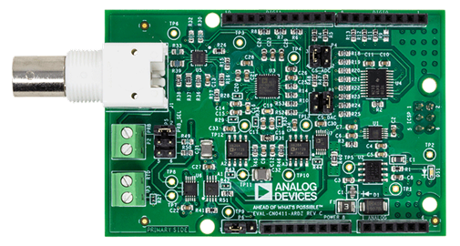
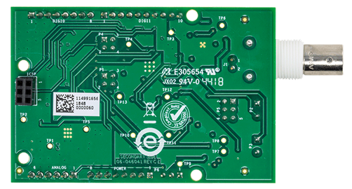
The circuit setup for the CN-0411 consists of the EVALCN0411-ARDZ evaluation board and the EVAL-ADICUP360 board. The EVAL-CN0411-ARDZ comes in an Arduino shield form factor, making it possible to use additional pin compatible developments boards for evaluation and prototyping. The CN-0411 demo software (see the CN-0411 Software User Guide for complete details) allows the EVAL-ADICUP360 board to configure and read data from the EVAL-CN0411-ARDZ evaluation board. This data can be displayed using a serial port terminal program on a PC.
Equipment Needed
The following equipment is needed:
- PC with a USB port and Windows® 7 (32-bit) or higher
- EVAL-CN0411-ARDZ circuit evaluation board
- EVAL-ADICUP360 development board
- CrossCore Embedded Studio
- Micro-USB to USB connector
- 2-wire conductivity cell with RTD
Getting Started
- A detailed user guide for the EVAL-CN0411-ARDZ is available at www.analog.com/CN0411-UserGuide. Consult this user guide for all details and aspects of hardware and software operation.
- A detailed user guide for the EVAL-ADICUP360 platform board is also available at www.analog.com/EVAL-ADICUP360
- Set the jumpers on the EVAL-ADICUP360 board and the EVAL-CN0411-ARDZ board to the positions indicated in the CN-0411 User Guide.
- Download the CN-0411 demo code to the EVAL-ADICUP360 board using the CrossCore Embedded Studio and DEBUG USB connection.
- Connect the EVAL-CN0411-ARDZ board to the EVALADICUP360 using the mating headers. Connect your conductivity cell and RTD to the BNC connector and/or terminal blocks provided on the EVAL-CN0411-ARDZ board.
- Connect the USER USB port of the EVAL-ADICUP360 to the PC. On the PC, start the preferred serial terminal software and connect to the EVAL-ADICUP360 serial port to begin reading the data.
- Other Arduino form-factor platforms can also be used to test and evaluate the EVAL-CN0411-ARDZ board. However, the software needs to be ported to the new processor/platform.
Test Setup Functional Block Diagram
A photograph of the sample test setup of TDS and conductivity measurement using the EVAL-CN0411-ARDZ circuit board and the EVAL-ADICUP360 board is shown in Figure 17.

A functional block diagram of the test setup is shown in Figure 18. A complete schematic of the evaluation board is contained in the CN-0411 Design Support Package, including layout, Gerber files, and a bill of materials.

Test Setup
To measure electrical conductivity and TDS of a solution sample, take the following steps:
- Connect the sensor probe to the CN-0411 system either through the BNC connector if it is available or wired through the terminal block P2. Connect the conductivity probe’s RTD wires to terminal block P3.
- Dip the probe into the solution sample preferably at the center of the container to maximize the accuracy of the conductivity cell.
- Set the cell excitation voltage and operating frequency through serial commands from the terminal software
- Set the conductivity probe cell constant and select the type of solution and the conversion mode of the ADC. For a detailed description of these settings, see the CN-0411 User Guide.
- Follow the prompts on the serial terminal to perform conductivity or TDS measurements. Additionally, calibration routines may be performed before any measurement. See the CN-0411 User Guide for the detailed procedure for calibration.
The performance of the circuit can also be tested without the conductivity cell and sample solutions by using a precision resistor of known value.
Hardware and software operation details are available in the CN-0411 User Guide at www.analog.com/CN0411-UserGuide.
