AN-1531: Measuring −48 V High-Side Current Using the AD629 Difference Amplifier, AD8603 Op Amp, AD780 Reference, and AD7453 12-Bit ADC Single-Supply Components
Circuit Function and Benefits
The −48 V power rail is widely used in wireless base stations and telecommunication equipment. Used in network central offices, the voltage of the power rail can vary between −48 V and −60 V. Measuring the current at these voltages typically requires components that operate on dual supplies, such as ±15 V. Typically, only the front-end conditioning amplifiers that interface directly with the −48 V rail use dual supplies. The remainder of the system operates on single supplies. Eliminating the negative supply reduces complexity and cost. Using the AD629 and the AD8603 in the circuit shown in Figure 1 allows users to measure current at −48 V to −60 V while operating only on positive supplies.
Compared with low-side current sensing, high-side current sensing rejects ground noise and can detect short circuits during operation.

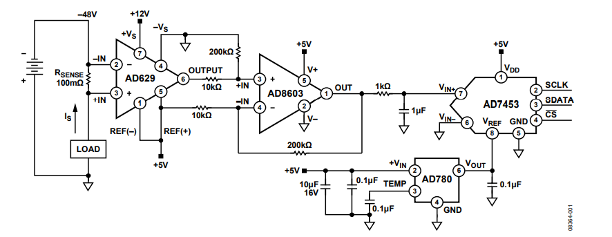
Circuit Description
This circuit uses the AD629 difference amplifier to condition voltages beyond its supplies. The minimum and maximum allowable input common-mode voltage is determined by the following equations:
VCOM_MAX = 20 × (+VS − 1.2) − 19 × VREF
VCOM_MAX = 20 × (−VS + 1.2) − 19 × VREF
where:
VCOM_MAX is the common-mode voltage, maximum.
+VS is the positive supply voltage.
VREF is the reference voltage
VREF is the reference voltage
VCOM_MIN is the common-mode voltage, minimum.
−VS is the negative supply voltage.
When VREF = 5 V, +VS = 12 V, and −VS = 0 V, the AD629 commonmode input range is −71 V to +121 V. This range is high enough to cover the entire expected range of the −48 V rail. The AD629 difference amplifier senses the differential voltage, sense current (IS) × sense resistor (RSENSE), which is generated by the current flowing through the shunt resistor. Because the AD629 has a fixed gain of 1, its output voltage is equal to IS × RSENSE + VREF.
The shunt resistor is 100 mΩ with 0.1% tolerance and a maximum power rating of 1 W. When selecting the shunt resistor, both current measurement accuracy and self heating effects must be considered.
The AD8603 is configured as a subtractor so that it can reject the 5 V common-mode voltage and amplify the signal of interest, IS × RS. The signal is amplified by a factor of 20 to span the 2.5 V full-scale input range of the AD7453 analog-to-digital converter (ADC). A full-scale 2.5 V signal to the ADC corresponds to a current of 1.25 A on the −48 V supply. The AD8603 is selected for this circuit because it has low input bias current, low input offset drift, and rail-to-rail input and output features. The railto-rail output allows the AD8603 to share the same supply as the ADC. Note that the output of the AD8603 can only decrease to approximately 50 mV above ground due to its output stage. This output corresponds to a sense current, IS, of about 25 mA. Therefore, currents less than about 25 mA cannot be measured. However, accuracy for very low currents is not usually required.
The ratios of the four resistors that form the subtractor must be matched to obtain maximum common-mode rejection (CMR). In this stage, the subtractor has to reject the 5 V common-mode signal from the AD629.
The AD7453 12-bit ADC is used because of its pseudo differential input that can simplify the interface between the AD8603 and the ADC. In addition, its small package and low cost make it useful in cost sensitive or size limited cases.
The AD780 is used as the voltage reference for the AD7453 12-bit ADC because of its accuracy and ease of use.
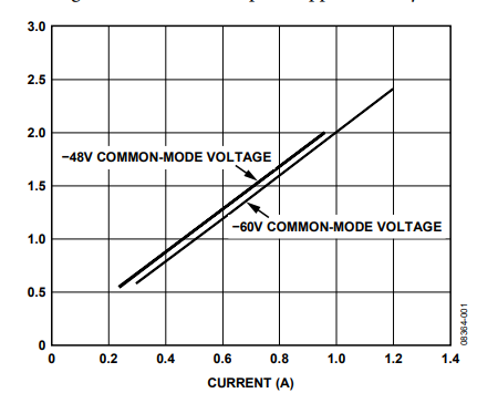
The circuit was tested by measuring the digitized output voltage as a function of current for supply rails of −48 V and −60 V. The results shown in Figure 2 demonstrate a close correlation to the expected values and good linearity under different commonmode voltages.

The error due to the CMR of the AD629 is the largest error. The total offset error is amplified by the signal gain of the AD8603 difference amplifier, 20; therefore, the total offset error can be as high as 156 mV referenced to the AD8603 output.
This calculation shows that the CMR of the input difference amplifier is important for low offset. If the current sense circuit is used outdoors, the temperature specifications (initial gain drift, offset voltage drift, and CMR over the entire temperature range) are important, and the AD629 is ideal for such applications.
The AD8603 contributes an error caused by its input offset voltage (0.3 mV maximum) and input bias current (1 pA). These amplifier errors produce a maximum output offset error of about 6.3 mV for the noise gain of 21. The total maximum output offset error is the sum of the error due to the AD629 (156 mV) and the AD8603 (6.3 mV), or 162.3 mV referred to the AD8603 output. Remove this error with system calibration.
If using the typical specifications rather than maximums, the offset voltage at the AD8603 output is approximately 45 mV.
The offset errors of the AD629A are shown in Table 1 and can be calculated as follows using the maximum specifications.
| Error Source 1 | Error Voltage (mV) |
| Initial Gain Error | 0.05 |
| Offset Voltage | 1 |
| DC CMR (77 dB) | 6.768 |
| The total offset error voltage of these error sources is 7.818 mV. | |
The circuit must be constructed on a multilayer printed circuit board with a large area ground plane. Proper layout, grounding, and decoupling techniques must be used to achieve optimum performance (see the MT-031 Tutorial, Grounding Data Converters and Solving the Mystery of “AGND” and “DGND” and MT-101 Tutorial, Decoupling Techniques).
Common Variations
The ADR361 is another option for the voltage reference because of its smaller size, low power, and high precision.
An integrated instrumentation amplifier, such as the AD8223 or AD8226, can be used instead of the AD8603. This amplifier eliminates the need for the external resistor matching required by the AD8603 circuit. A difference amplifier, such as the AD8276 with integrated resistors, can also be used instead of the AD8603 if a gain of 1 is acceptable.
The AD629B has a CMR that is 9 dB higher than the AD629A. Its offset voltage is half and its gain error is almost half that of the AD629A. These specifications are critical for cases where system calibration is impossible.
If a more integrated solution is needed for the converter, the ADuC7019, ADuC7020, ADuC7021, ADuC7022, ADuC7024, ADuC7025, ADuC7026, ADuC7027, and ADuC7028 series of ARM7TDMI® precision analog microcontrollers with the integrated 12-bit, 1 MSPS ADC are ideal choices.
References
Kitchin, Charles and Lew Counts. 2006. A Designer's Guide to Instrumentation Amplifiers (3rd Edition). Analog Devices.
MT-035 Tutorial, Op Amp Inputs, Outputs, Single-Supply, and Rail-to-Rail Issues. Analog Devices.
MT-061 Tutorial, Instrumentation Amplifier (In-Amp) Basics. Analog Devices.
MT-068 Tutorial, Difference and Current Sense Amplifiers. Analog Devices.